Abstract
The function of rapid thermal annealing on zinc-diffused In0.53Ga0.47As/InP PIN detector was systemically studied. By using electrochemical capacitance-voltage and secondary ion mass spectroscopy techniques, Zn and net acceptor concentration profiles were investigated, indicating that the annealing process would affect the dopant concentration but not affect the diffusion depth. In0.53Ga0.47As/InP PIN detectors under different annealing conditions were fabricated, the results showed that the detector without annealing process outperformed in terms of lower device capacitance and higher activation energy from 260 to 300K. By analyzing the mechanism of dark current, the unannealed sample exhibited lower Shockley-Read-Hall generation-recombination and diffusion currents, explaining the higher peak detectivity at room temperature. Therefore, for the purpose of fabricating high-performance planar InGaAs detectors with low-doped absorption layer, annealing process is inadvisable.Introduction
The shortwave infrared(SWIR)waveband has traditionally been defined as the spectral region between 1 μm and 3 μm[1]. As one of the "atmospheric windows",the photodetectors(PDs)responding to SWIR waveband can receive more radiation energy and gain unique spectral features,such as the water molecules,CO2,etc[2]. In addition,SWIR detecting and imaging is based on the reflection imaging from the target,consequently it is typical of the distinct detail resolution ability that medium and long wavelength infrared imaging lack[3].
In recent years,SWIR detection systems are increasingly demanded for surveillance,reconnaissance,and remote sensing applications[4-6]. Lattice-matched In0.53Ga0.47As/InP have a response from 0.9-1.7 μm at room temperature(RT),which coincides extremely well with peaks in the ambient nightglow. Due to the very low photon flux levels of the starlight and nightglow,dark current and noise characteristics of the detector have a direct influence on the imaging capability under low light level condition[7-9].The electrical noise of the FPA is mainly determined by the capacitance of the photodiode,especially in the case of short integration time,large integration capacitance,and small pixel pitch[10]. In general,the detectors with lower concentration absorption layer tend to have a wider depletion region and a lower capacitance. For lattice-matched InP-based material,planar-type devices have been the main stream. The p-n junctions of planar devices were prepared by using p-type impurity diffusion process[11].It is important to understand and optimize the diffusion process which significantly affects the photoelectric performance of the detector. Some previous studies have revealed that the p-type impurity diffusion technique had a common feature in low activation efficiency[12-14]. Since that,rapid thermal annealing is considered as the effective process for obtaining high hole concentrations. It’s identified that after annealing in Nitrogen atmosphere,the net acceptor concentration in the diffused InP increases by one order of magnitude[15].These works were mostly focused on the middle-doped(>5×1015 cm-3)material system[12-16]. However,the effect of rapid thermal annealing on InGaAs/InP devices with low-doped(<1×1015 cm-3)absorption layer still lacks research.
In this work,the function of rapid thermal annealing on zinc-diffused In0.53Ga0.47As/InP PIN detector was systemically studied. The pn junction in the InP/InGaAs heterostructure was prepared by sealed-ampoule Zn diffusion. The profiles of Zn and acceptor concentration before and after thermal annealing were investigated. By analyzing thermal activation energy and the mechanism of dark current,we explained lower dark current of the unannealed In0.53Ga0.47As/InP PIN detector.
1 Experiments
In experimental section,the n-i-n+ InP/InGaAs/InP epitaxy layers were grown on an n-type heavily doped InP substrate by metal-organic chemical vapor deposition(MOVCD)system. The epitaxial structure consisted of a 1 µm n-InP cap layer with electron concentration of 5×1016 cm-3,a 2.5 µm low-doped In0.53Ga0.47As absorption layer with electron concentration of 2×1014 cm-3 and a 1 µm highly Si-doped InP buffer layer with electron concentration of 2×1018 cm-3. The parameters of the as-prepared epitaxy material are given in Tab. 1.
| Sample Number | A | B | C | D |
|---|
| Diffusion temperature/℃ | 530 | 530 | 530 | 530 |
| Diffusion time/min | 10 | 10 | 10 | 10 |
| Annealing temperature/℃ | 450 | 450 | 450 | 450 |
| Annealing time/min | 0 | 3 | 7 | 10 |
Table 2. Conditions of diffusion and annealing process for detectors
| Epitaxy layer | Layer thickness/μm | Doping concentration/cm-3 |
|---|
| n-InP capping layer | 1 | 5×10¹⁶ |
| i-In0.53Ga0.47As absorption layer | 2.5 | 2×10¹⁴ |
| n+-InP buffer layer | 0.5 | >2×10¹⁸ |
| InP substrate | 350 | >4×10¹⁸ |
Table 1. The PIN epitaxy materials for detectors
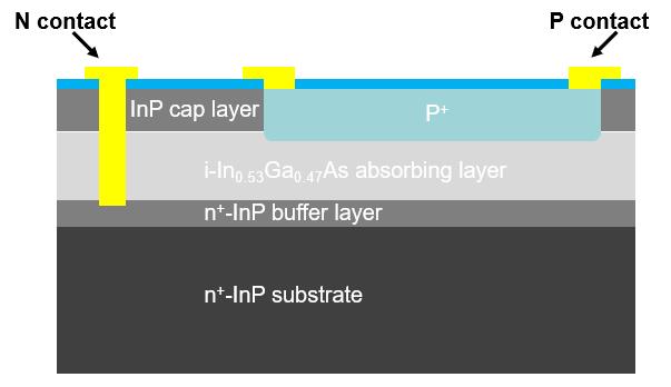
To form P-well in the cap layer,the Zn diffusion processes were implemented via sealed-ampoule technique. After diffusion,rapid thermal annealing treatment was performed on AccuThermo AW610 Rapid Thermal Processing System in N2 atmosphere. The variations of different annealing process are shown in Table 2. The metal deposition and contact pads preparation were accomplished in sequence. The schematic diagram of the planar PIN photodiode is shown in Fig. 1. The optical microscopy image of the diode is shown in Fig. 2.

Figure 1.Cross-section diagram of the PIN planar type photodiode
Figure 2.The optical microscopy image of Φ1 mm detector
Zn diffusion depth was measured by electrochemical capacitance-voltage(ECV)depth profiling and by secondary ion mass spectroscopy(SIMS). In ECV characterization,a Schottky barrier is formed between the interface of semiconductor and an electrolyte,while capacitance-voltage measurements are used to determine the doping type and concentration. Carrier depth information is obtained by using calibrated anodization and dissolution[17]. For the measurement of SIMS,the CAMECA 7f-auto instrument was applied. Zn elements depth profiles were obtained with 9keV Cs+ beam using the CsZn+ cluster at mass 197 as the analytical ion. The sputtered area was 200 μm × 200 μm with the analyzed area of 60 μm diameter. SIMS is sensitive to the total chemical concentration,not the active carrier concentration[18]. The photoluminescence(PL)signals were detected by a Bruker VERTEX 80v Fourier transform infrared(FTIR)spectrometer. 532 nm laser and 1064 nm laser were applied for the different response wavelength of each epitaxial layer.
The current-voltage(I-V)and capacitance-voltage(C-V)characteristics were measured by Agilent B1500A Semiconductor Device Analyzer. For the response characteristic,the blackbody response signal and total dark noise measurements were conducted by using a blackbody testing setup with a blackbody temperature of 900 K,a distance of 30 cm,and an aperture of 8 mm. Spectral responsivities were measured by using a Fourier spectrometer at RT.
2 Results and discussions
2.1 Zn diffusion profiles
Due to the limited characterization capability of SIMS and ECV on the micrometer-scale samples,sealed-ampoule diffusion was carried out on planar InP/InGaAs epitaxial wafer. Net acceptor concentration profiles were measured by the ECV technique as shown in Fig. 3. The ECV profile indicated the net acceptor concentration in InP varies from 7×1017 cm-3 to 1.5×1018 cm-3 before and after annealing. For the annealed sample,the value of the net acceptor concentration in InP is close to the solubility limit of Zn doping by metal organic vapor phase diffusion[13].Also,one order magnitude increase(from 2.7×1018 cm-3 to 3.2×1019 cm-3)of net acceptor concentration in InGaAs layer was observed,which is consistent with the previous report of semi-closed ampoule Zn diffusion[16]. Considering the different solubility of Zn in InP and InGaAs,the rapid thermal annealing process exacerbates the difference of diffusion behavior in each layer.
Figure 3.Net acceptor concentration profiles measured by ECV
Fig. 4 shows Zn concentration profiles measured by SIMS. It is obvious that by using sealed-ampoule diffusion the Zn concentration of 4.4×1018 cm-3 were much higher than the net acceptor concentration of 7×1017 cm-3. According to the previous studies,low activation efficiency of acceptor in InP can be attributed to the interstitial-substitutional diffusion model,in which the fast-diffusing interstitial species is un-ionized[12,19-20].Both ECV and SIMS data showed the accumulation of acceptor and Zn concentration at InGaAs/InP heterojunction around 1.1 μm depth. It is noteworthy that the diffusion depth was independent with the rapid thermal annealing process.
Figure 4.Zn concentration profiles measured by SIMS
Moreover,the annealed sample exhibited more uniform Zn element distribution in InP cap layer as shown in Fig. 4. From the perspective of net acceptor concentration,which affects the ohmic contact,unannealed sample exhibited similar uniformity,as shown in Fig. 3. Due to the lower diffusion coefficient of Zn in InGaAs,the accumulation of Zn on the interface of heterojunction was expected [18]. Although with slightly decrease in the net acceptor concentration for the unannealed sample,the dopant accumulation around the InGaAs/InP junction region was suppressed in large extent,which may benefit the photodiode performance.
2.2 PL measurements
By using 532 nm laser,the laser continuously excites the electron-hole pairs in the InP cap layer,while the excited carriers are also continuously recombined to emit light. When the lifetime is long enough,the excited electron-hole pairs will be driven by concentration gradient to diffuse to the InGaAs layer,and then are recombined to emit light. By using 1064 nm laser,InP cap layer can not absorb the light in this band,since the incident light reach the InGaAs layer without loss in InP cap layer. The InSb near-infrared detector was adopted to detect the photoluminescence of the InGaAs layer,so 532 nm laser and 1064nm laser were actually applied to test the performance of the epitaxial layers and the InGaAs layer,respectively. PL spectrum at different laser wavelength were measured at RT,as shown in Fig. 5. At 532 nm and 1064 nm laser wavelength,PL intensity of the as-grown epitaxial material monotonically decreased for both unannealed and annealed samples. After diffusion and the subsequent annealing,the non-radiative recombination rate of the epitaxial material increased while the radiative recombination rate decreased. This can be explained that the dopant diffuses into the layers and forms impurity energy levels,causing more non-radiative recombination centers,then dramatically reducing the PL intensity. Notably,the photoluminescence performance of the surface-exposed InP cap layer will decrease in higher level. In other words,this will directly cause more drastic decrease of PL intensity at 532 nm in Fig. 5(a)after diffusion and annealing process. By means of PL measurement,it is testified that rapid thermal annealing process allows more Zn atoms to reach the lattice site forming activated acceptors[21].
Figure 5.PL spectrum of samples with different probe laser wavelengths:(a)only 532 nm probe;(b)only 1064 nm probe
2.3 Detector capacitance analysis
Reverse bias-dependent capacitances(Cd)of the photodiodes with and without rapid thermal annealing were characterized at RT,as shown in Fig. 6. Monotonically decreased Cd Curves with the increase of the reverse bias were observed. The zero bias junction capacitance is 24.4 pF for the unannealed PD,6% lower than the annealed PD. This trend remained consistent for reverse biases up to 1V. C-V measurements for both PDs were also performed on a number of devices to exclude the possibility of experimental uncertainties and to ensure the reliability and reproducibility of the data.
Figure 6.Measured Cd-V curves of the unannealed PD and annealed PD
The capacitance density of the p+n abrupt junction can be represented by ,and thus ,where εs is the dielectric constant,Vbi is the built-in voltage,NBis the doping concentration of the absorption layer. The capacitance density of linearly graded junction can be represented by ,and thus ,where ajis the concentration gradient[22]. The curves and corresponding linear fitting curves of the unannealed PD and annealed PD were shown in Fig. 7. Obviously,the well-fitted linearity of the data indicated the impurity concentration distribution of the low-concentration device was more corresponding to the linearly graded junction than the abrupt junction. For the unannealed PD,the fitted concentration gradient of absorption layer is 1.1×1019 cm-4,which is calculated according to ,where εs is the dielectric constant,q is the electronic charge and the slope is extracted from the linear fitting curve. For the annealed PD,the fitted concentration gradient is 1.3×1019 cm-4. Considering the identical parameters of the materials and processes for both samples,the increasement of impurity concentration gradient for the annealed PD should be recognized as the result of the carrier accumulation(in Fig. 3)around the heterojunction interfaces.
Figure 7.The Cd-3-V curves and corresponding linear fitting curves of the unannealed PD and annealed PD
2.4 Dark current analysis
For photodetectors,dark current is the key parameter which must be decreased to improve signal to noise ratio and then minimize the noise equivalent power[23]. Typically,under reverse bias voltage,dark current Id of the planar InGaAs photodiodes is composed of four main components,that is,diffusion current Idiff,Shockley Read Hall(SRH)generation-recombination current Igr,shunt current Ish and tunneling current Itun. Diffusion current is attributed to the carrier gradients within the material. SRH generation-recombination current primarily originates in the depletion region of the lower bandgap InGaAs,which is proportional to the depletion region width and reverse bias. Shunt current spreads through defects under the top passivation and at the InGaAs/InP interface[24-25]. Since low reverse bias was applied in this study,diffusion,SRH generation-recombination and shunt currents are taken into account.
Dark current-voltage(I-V)measurements were carried out in a cryogenic probe station which was connected to a precision semiconductor parameter analyzer and also precisely controlled the chamber temperature. Figs. 8(a)-(e)showed the measured temperature-dependent I-V curves for Φ1mm diodes with different annealing conditions under 260-300K. The measured dark currents at -100 mV(300 K)were 69.8,91.8,108 and 112 pA for the annealing time of 0,3,7 and 10 min,respectively. The dark currents at -100 mV(260K)were 0.99,1.70,1.74 and 2.01 pA for the annealing time of 0,3,7 and 10 min.
Figure 8.Measured dark currents for Φ1 mm detectors with different annealing time raging form 260K to 300K:(a)260K;(b)270K;(c)280K;(d)290K;(e)300K
Dark current mechanisms are dominated by diffusion current when Ea= Eg,whereas dominated by SRH generation-recombination current and shunt current when Ea= Eg/2. The energy bandgap Eg of In0.53Ga0.47As is 0.735eV at 300 K. In the following discussion,the weak energy bandgap change with temperature is ignored. Arrhenius plots of the temperature-dependent dark currents at different reverse-bias voltages for the unannealed PD and the annealed PD were shown in Figs. 9(a)and(b),respectively. By fitting the data,thermal activation energy Ea of both PDs were obtained,as listed in Table 3.
Figure 9.The dark current density as a function of 1000/T at different reverse-bias voltage for Φ1 mm detectors of different annealing time:(a)annealing 0 min;(b)annealing 10 minTable 3 The thermal activation energy Ea of the unannealed PD and the annealed PD
| unannealed PD | annealed PD |
|---|
| Ea(eV)@-0.5V | 0.637 | 0.587 |
| Ea(eV)@-0.4V | 0.653 | 0.610 |
| Ea(eV)@-0.3V | 0.671 | 0.616 |
| Ea(eV)@-0.2V | 0.692 | 0.639 |
| Ea(eV)@-0.1V | 0.715 | 0.680 |
| Ea(eV)@-0.01V | 0.718 | 0.687 |
Table 3.
At 260-300 K,the Ea of the unannealed PD was constantly higher than that of the annealed PD at different reverse-bias voltages,which indicates that non-diffusion current accounts for a larger proportion for the annealed PD. Also,the Ea gradually decreased for both PDs as reverse bias voltage increased. Since diffusion current is solely saturate at relatively high reverse bias,SRH generation-recombination current increases with the widened depleted region.
The dark currents measured and fitted for the unannealed PD and the annealed PD at 300K were showed in Fig. 10. For both PDs,the dark current mechanisms were dominated by diffusion current at relatively low reverse bias voltage,while the shunt current and the SRH current increased at relatively high reverse bias voltage. Moreover,the results also showed that the SRH current and diffusion current of the unannealed PD are lower compared with the annealed PD.
Figure 10.Dark current measured at 300K and fitted for Φ1 mm detectors of different annealing time:(a)annealing 0 min;(b)annealing 10 min
2.5 Spectral response and peak detectivity
To analyze the impacts of the rapid thermal annealing on photoelectric detection,spectral response and detectivity were also investigated. The as-prepared separate detectors with different annealing conditions were packaged in Dewars for the measurement. The spectral response of the detectors was carried out by a Fourier transform infrared spectrometer at room temperature under zero bias as seen in Fig. 11. The peak response is at 1.56 μm,with 50% cutoff wavelength of 1.69 μm. The unannealed detector exhibited higher spectral responsivity over the annealed sample,as shown with black line.
Figure 11.The detectivity spectrum of detectors at 300K
Peak wavelength detectivity(D*)represents the sensitivity of the photosensitive element of the detector under unit bandwidth area and per unit radiation power. The RT response signal and dark noises under zero bias were also acquired by using a lock-in amplifier with a ×108 voltage preamplifier under a 900 K blackbody radiation chopped at 800 Hz,from which the peak D* were deduced. The calculated peak detectivity of the unannealed detector is 6.2×10¹² cmHz1/2W-1,obviously higher than the annealed detector with the value of 5.7×10¹² cmHz1/2W-1 at RT. Such results clearly proved that the unnecessity of rapid thermal annealing treatment for the InGaAs/InP PIN detector with low-doped absorption layer.
3 Conclusions
In this work,the function of rapid thermal annealing on In0.53Ga0.47As/InP PIN detector with low-doped absorption layer was investigated. The results of SIMS and ECV showed that the dopant accumulation around the InGaAs/InP junction region was directly affected by annealing after Zn diffusion. The capacitance-voltage measurement revealed that impurity concentration distribution of the linearly graded junction in InGaAs layer and the lower capacitance of the unannealed detector. Moreover,the unannealed detectors has a lower dark current in the full temperature range,benefiting from the suppressed dopant accumulation. The fitting results indicated the annealed detector has higher SRH current and diffusion current. The peak detectivity of the unannealed detector is 6.2×10¹² cmHz1/2W-1,8.8% higher than that of the annealed sample. Therefore,for the purpose of fabricating high-performance planar InGaAs detectors with low-doped absorption layer,annealing process is inadvisable.
References
[1] T Martin, R Brubaker, P Dixon et al. 640×512 InGaAs focal plane array camera for visible and SWIR imaging. Proc SPIE, 5783, 12-20(2005).
[2] Yong-Gang Zhang, Gu Yi, Li Xue et al. Short-wave infrared InGaAs photodetectors and focal plane arrays. Chinese Physics B, 27, 128102-128102(2018).
[3] M H Ettenberg, M A Blessinger, M T O'Grady et al. High-resolution SWIR arrays for imaging at night. Proc SPIE, 5406, 46-55(2004).
[4] H Figgemeier, M Benecke, K Hofmann et al. SWIR detectors for night vision at AIM. International Society for Optics and Photonics(2014).
[5] R H Vollmerhausen, T Maurer. Night illumination in the visible, NIR, and SWIR spectral bands. Proc SPIE, 60-69(2003).
[6] R Littleton,, Bellotti et al. Electro-Optical Characteristics of P+n In0.53Ga0.47As Hetero-Junction Photodiods in Large Format Dense Focal Plane Arrays. Journal of Electronic Materials, 44, 2813-2822(2015).
[7] P D Levan, A K Sood, P Wijewarnasuriya et al. SWIR detectors for low photon fluxes. Infrared Sensors, Devices, and Applications VI, 9974, 99740G(2016).
[8] B.F. Andresenet al. Low dark current small pixel large format InGaAs 2D photodetector array development at Teledyne Judson Technologies. Proc SPIE, 835309, 1-8(2012).
[9] D Andrew. Hoodet al. Large-format InGaAs focal plane arrays for SWIR imaging, Proc SPIE, 83530A, 1-7(2012).
[10] Chun-Lei Yu, Xue Li, Bo Yang et al. Noise Characteristics Analysis of Short Wave Infrared InGaAs Focal Plane Arrays. Infrared Physics & Technology, 85, 74-80(2017).
[11] Hao Yin, Yong-Fu Li, Wen-Juan Wang et al. Scanning capacitance microscopy characterization on diffused p-n junctions of InGaAs/InP infrared detectors. Proc SPIE, 7658, 237-238(2010).
[12] G Gurp, T V Dongen, G M Fontijn et al. Interstitial and substitutional Zn in InP and InGaAsP. Journal of Applied Physics, 65, 553-560(1989).
[13] A V Geelen, T Smet, T V Dongen et al. Zinc doping of InP by metal organic vapor phase diffusion (MOVPD). Journal of Crystal Growth, 195, 79-84(1998).
[14] G M Fontijn, G Gurp, K Janssen et al. The behaviour of Zn in InP and InGaAsP studied by SIMS. Ultramicroscopy, 27, 204-204(1989).
[15] Gao-Qi Cao. Study on high sensitivity planar InGaAs short wavelength infrared detector(2016).
[16] Su-Xiang He, Yan-Li Zhao. An experimental investigation of Zn diffusion into InP and InGaAs. Semiconductor Science and Technology, 20, 149-151(2005).
[17] U Schade, P Enders. Rapid thermal processing of zinc diffusion in indium phosphide. Semiconductor Science and Technology, 7, 752-757(1992).
[18] M H Ettenberg, M J Lange, A R Sugg. Zinc Diffusion in InAsP/InGaAs Heterostructures. Journal of Electronic Materials, 28, 433-1439(1999).
[19] G V Gurp, P R Boudewijn, M Kempeners et al. Zinc diffusion in n‐type indium phosphide. Journal of Applied Physics, 61, 1846-1855(1987).
[20] B Tuck, A Hooper. Diffusion profiles of zinc in indium phosphide. Journal of Physics D Applied Physics, 8, 1806(1975).
[21] J K Hsu, C Juang, B J Lee et al. Photoluminescence studies of interstitial Zn in InP due to rapid thermal annealing. Journal of Vacuum Science & Technology B Microelectronics & Nanometer Structures, 12, 1416-1418(1994).
[22] E K Liu, B S Zhu, J S Luo et al. The Physics of Semiconductors(2003).
[23] R Dewames, R Littleton, K Witte et al. Electro-Optical Characteristics of P+n In0.53Ga0.47As Hetero-Junction Photodiodes in Large Format Dense Focal Plane Arrays. Journal of Electronic Materials, 44, 2813-2822(2015).
[24] B M Onat, H Wei, N Masaun et al. Ultra-low dark current InGaAs technology for focal plane arrays for low-light level visible-shortwave infrared imaging(2007).
[25] J A Trezza, N Masaun, M Ettenberg. Analytic modeling and explanation of ultra-low noise in dense SWIR detector arrays. Proc SPIE, 2(2011).