
Yuwei Nie, Wei Li, Jiagang Lü, Zhipeng Pan, Suping Liu, Xiaoyu Ma. Oxidation-Limited 795 nm Vertical Cavity Surface Emission Laser[J]. Chinese Journal of Lasers, 2024, 51(6): 0601004
- Chinese Journal of Lasers
- Vol. 51, Issue 6, 0601004 (2024)
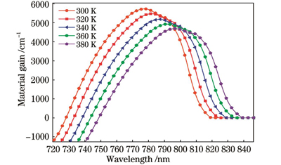
Fig. 1. Gain spectra of In0.08Ga0.79Al0.13As quantum-well at different temperatures
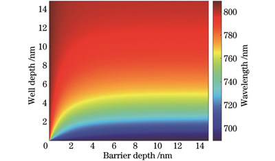
Fig. 2. Lasing wavelengths under different quantum well depths and barrier depths
Fig. 3. Reflection and transmission spectra of DBR. (a) Top DBR; (b) bottom DBR
Fig. 4. Schematics of oxidation limiting layer with gradient structure
Fig. 5. Electric field distributions of first 5 order transverse modes
Fig. 6. Transverse mode numbers of VCSELs with different oxidation apertures
Fig. 7. Current density and temperature distributions. (a) Current density and temperature distributions of single-tube VCSEL;(b) current density and temperature distributions of VCSELs with different oxidation apertures
Fig. 8. Structural diagram of oxidation confined top emission VCSEL
Fig. 9. Test results of epitaxial sheet. (a) Photoluminescence spectrum; (b) cavity mode; (c) reflection spectrum
Fig. 10. Table design drawings and physical drawings of lithographic masks. (a) Design drawings; (b) physical drawings
Fig. 11. Preparation process of VCSEL device. (a) Mesa etch; (b) wet oxidation; (c) deposition of dielectric film; (d) P-surface electrode preparation; (e) substrate thinning; (f) N-surface electrode preparation
Fig. 12. Oxidation apertures of prepared VCSEL devices
Fig. 13. Physical image of VCSEL
Fig. 14. Power-current curves of VCSELs with different oxidation apertures
Fig. 15. Spectra of VCSELs with different oxidation apertures
Fig. 16. Spectra of VCSELs with different oxidation apertures under different driving currents. (a) Oxidation aperture of 1.9 μm;(b) oxidation aperture of 3.8 μm

Set citation alerts for the article
Please enter your email address
© Copyright 2018-2021 | Chinese Laser Press. All Rights Reserved 沪ICP备15018463号-20