
Guohua Hu, Zhipeng Qi, Binfeng Yun, Ruohu Zhang, Yiping Cui. Compact, integrated PLZT optical switch array[J]. Chinese Optics Letters, 2015, 13(11): 111301
- Chinese Optics Letters
- Vol. 13, Issue 11, 111301 (2015)
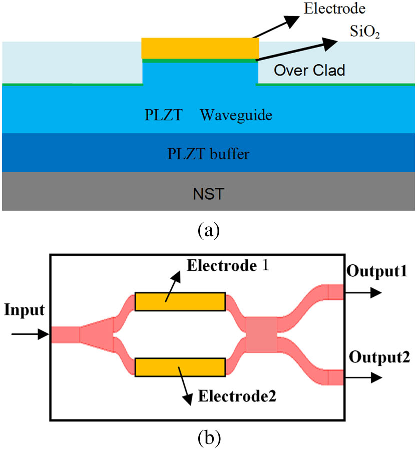
Fig. 1. Schematic of
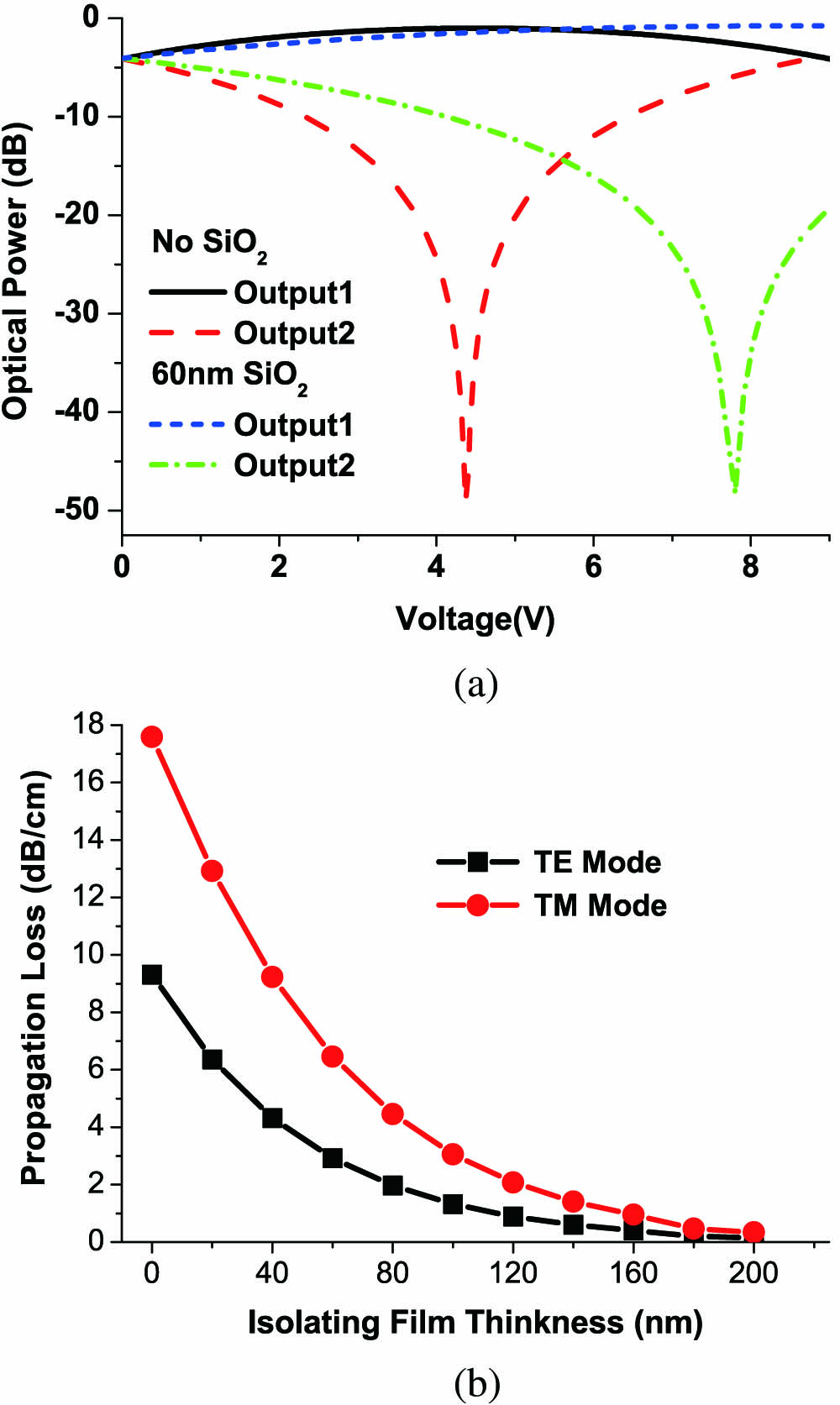
Fig. 2. Simulation results of the switches. (a) Voltage response of
Fig. 3. Schematic of PLZT optical switch array. (a) The conventional cascaded structure. (b) The proposed cascaded structure.
Fig. 4. PLZT optical switches chip. (a) Scanning electron microscope etched waveguide. (b) The chip connected to the bond pad by Au interconnects.
Fig. 5. Voltage response of
Fig. 6. Switching time of
| ||||||||||||||||||||||||||||||
Table 1. Insertion Loss of 1×4 Switch Array

Set citation alerts for the article
Please enter your email address
© Copyright 2018-2021 | Chinese Laser Press. All Rights Reserved 沪ICP备15018463号-20