Abstract
Due to the excellent electro-optic properties of lead lanthanum zirconium titanate (, PLZT), compact and PLZT optical switches with a high response speed are proposed and fabricated successfully in this Letter. By introducing a thin isolating layer between the waveguides and the electrodes, the absorption loss of the fabricated PLZT switch caused by the electrodes is reduced 8.9 dB with a relatively low driving voltage. The PLZT switch shows an insertion loss of 18.3 dB and crosstalk of at an applied voltage of 9.5 V. The fabricated switch array shows an insertion loss of 20.7 dB and a crosstalk of at an applied voltage of 13 V. The response time of the switches is less than 27 ns, and the device’s size is only . The switches can be used in optical communication systems. (PLZT) is a kind of attractive material in terms of its high speed, low driving voltage, and small-sized optical waveguide switch due to its high electro-optical (EO) coefficient. It was reported that the EO coefficient of PLZT ceramic (8/65/35: , , ) film is as high as [1,2]. Optical switches fabricated based on PLZT waveguides with nanosecond speeds have been reported[3–7].
It is very useful to reduce the absorption loss by using the indium tin oxide (ITO) electrodes to replace the traditional metal electrodes. But when an ITO electrode is deposited on top of the waveguide directly[8], the absorption loss will increase. Adding a thick cladding layer between the waveguide and the electrode could prevent optical absorption by the electrode, but it will result in the requirement of a high driving voltage, as the dielectric constants of PLZT materials are hundreds of times higher than that of the conventional materials[9] (such as silica and polymer). In this Letter, by introducing a 60 nm silica isolating layer between the waveguides and the electrodes, both a compact size and a low insertion loss could be obtained. To realize the compact size of the switch array, a new type of cascaded structure is proposed here. With the amounts of switch units increasing to a switch array, the advantages of this new design will be more and more significant.
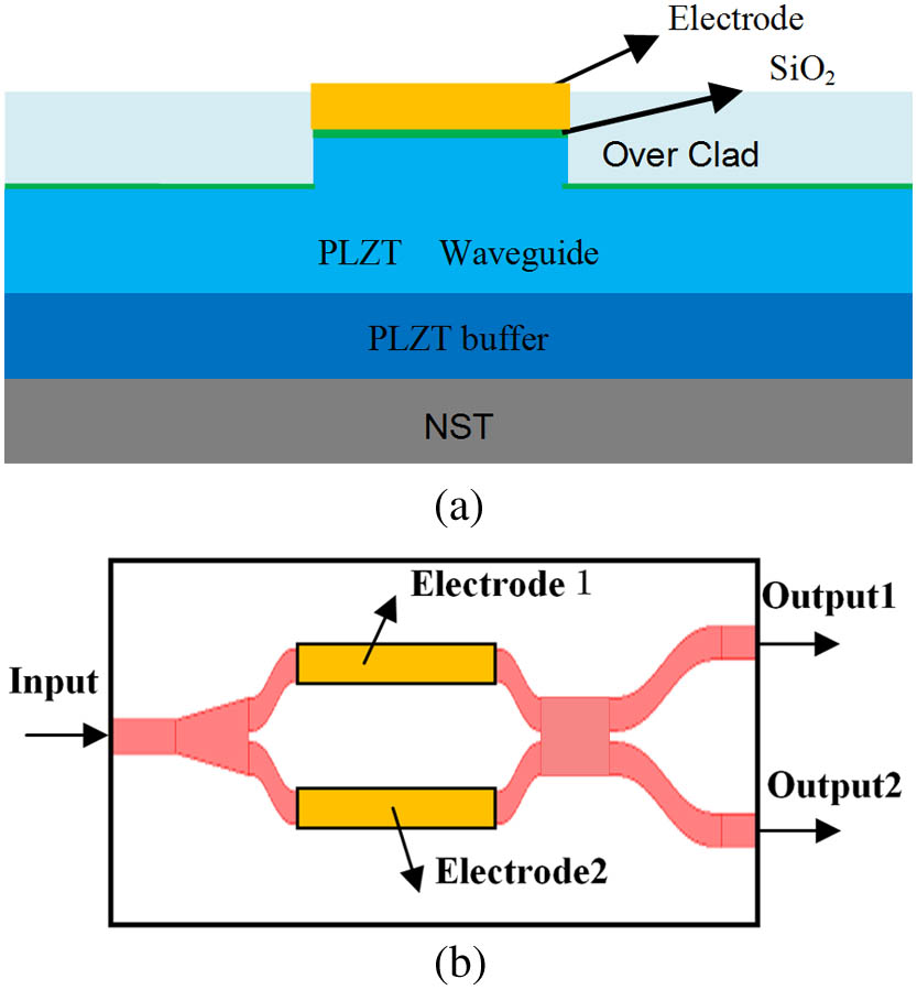
Figure 1(a) shows the cross-section of the designed PLZT switch. Niobium-doped strontium titanate (NST) is chosen as the substrate and for the bottom electrode as well. The thickness of the PLZT buffer layer is 2.6 μm, which is necessary to avoid absorption by the NST substrate[9]. The refractive index of the PLZT buffer film is 2.4086 for TM mode. The thickness of the PLZT waveguide layer is 2.35 μm, with a ridge height and width of 0.6 and 3.5 μm for single-mode propagation at 1550 nm according to the planar waveguide theory[10,11]. For the PLZT waveguide films, the refractive index is 2.4552 for TM mode (the refractive indices given for each section were measured at the wavelength of 1550 nm by using the prism coupler). The EO coefficient of the PLZT waveguide film is . The commercially available UV-curable perfluorinated acrylate material ZPU13-44 is used as the overclad layer. The refractive index is 1.44.
Sign up for Chinese Optics Letters TOC. Get the latest issue of Chinese Optics Letters delivered right to you!Sign up now

Figure 1.Schematic of PLZT MZI optical switch. (a) Cross-sectional view of PLZT waveguide. (b) Top view of MZI switch.
The schematic of the PLZT Mach−Zehnder interference (MZI)[12] optical switch is shown in Fig. 1(b). A linear tapered waveguide is introduced to connect the input and the two branch waveguides. Considering the conventional lithography resolution, the width of the branching gap[13] between two waveguides is set as 1.5 μm in our work. Because of its excellent properties and ease of fabrication, a multimode interference (MMI)-type coupler[14–16] could be used to improve the process tolerance. The length of the MMI coupler is set as , where [14]. and are the equivalent effective index and the width of the MMI waveguide. Here, , and the branching gap is also 1.5 μm. The length of the MMI coupler is determined to be 228 μm.
A three-dimensional finite-difference beam propagation method was used to simulate the switches. Figure 2(a) shows that the relationship between the applied voltage and the output optical power of the switches with or without isolating layers for the TM mode at a wavelength of 1550 nm. The excess loss introduced by the branch, MMI coupler, and arc bends is no more than 1 dB when the propagation loss and the coupling loss are neglected. It seems that, compared to the switch without the isolating layer, the proposed structure with the 60 nm layer does not cause the deterioration of the effective EO effect. The switching is obtained at a voltage of 7.8 V (it could satisfy the requirements of a low driving voltage). A crosstalk of is obtained by optimizing the length of the MMI-type coupler.
Figure 2.Simulation results of the switches. (a) Voltage response of PLZT optical switches. (b) The relationship between the isolating film thickness and the optical absorption by the electrodes.
According to Ref. [17], the relationship between the isolating film thickness and the optical absorption by the electrodes could be calculated [as shown in Fig. 2(b)]. The optical absorption by a 3 mm-long electrode will be reduced from 5.3 to 1.9 dB for TM mode. (The refractive index of ITO is at 1550 nm[18] with a resistivity of approximately ohm meters).
A conventional tree-type optical switch array composed of the cascaded switch units is shown in Fig. 3(a). The optical switch shown in Fig. 1 is used as the switch unit. The spacing of the output ports connected to the fiber array is set at 127 μm. Considering the bending loss, the length of the output -bend waveguides of the stage should be much longer than that of the stage . Using this conventional tree configuration, the length of a PLZT switch array is 16 mm. The length of a PLZT switch array is 26 mm. And the length of a PLZT switch array is longer than 38 mm (the bend channels are all within a radius of 10 mm to reduce the radiation loss). It is difficult to find an available NST wafer for such a large-scale switch array.
Figure 3.Schematic of PLZT optical switch array. (a) The conventional cascaded structure. (b) The proposed cascaded structure.
In this Letter, a compact tree-type optical switch array is proposed [as shown in Fig. 3(b)]. The spacing of the output ports connected to the fiber array is also 127 μm. The output -bend waveguides of each switch unit have been replaced by the short arc-type waveguides. The next stage will naturally extend along with the arc waveguide. The -bend waveguides are only used in the last stage. Using the designed compact tree configuration, the lengths of the PLZT, PLZT, and PLZT switch arrays are reduced to 10, 14, and 18 mm, respectively (the bend channels each have a radius of 10 mm). This compact cascaded structure has high potential for applications with strongly preferred and switches.
The PLZT buffer layer and the core layer of a commercial PLZT film were grown using solid-phase epitaxy[9] on a NST (100) single-crystal substrate. The PLZT films were patterned by a conventional photolithography technique using a positive photoresist with a thickness of 2.0 μm. The PLZT waveguide layer was dry etched by using a reactive ion etching system. During etching, 30 sccm of and 10 sccm of Ar gas were introduced into the etching chamber while the pressure was kept at 3.5 Pa and the radio frequency power at 150 W. The etched surface of the waveguide is shown in Fig. 4(a). After the etching, the photoresist was removed using acetone with ultrasonic agitation. The 60 nm layer was deposited onto the PLZT waveguides directly by magnetron sputtering. Then, the top ITO electrodes with Al were fabricated onto the surface of the layer using sputtering and a lift-off process. The edge facets were formed by the standard polishing process after cutting, and then the PLZT switches chip was bonded to the electronics board as shown in Fig. 4(b). Finally, the surfaces of the waveguides were covered with a ZPU series UV-curable perfluorinated acrylate material (ZPU 13-44) as the overclad layer. The and the switches and a straight ridge waveguide with the layer were fabricated on the same chip. The switch without the layer was also fabricated on another chip for comparison.
Figure 4.PLZT optical switches chip. (a) Scanning electron microscope etched waveguide. (b) The chip connected to the bond pad by Au interconnects.
A commercial laser with a wavelength of 1550 nm provides continuous-wave generation, which was launched into a single-mode fiber and connected to the input waveguide. The output waveguides of a fabricated switch were connected to the other two single-mode fibers. By applying a voltage to the top electrodes, the relationship measured between the applied voltage and the output optical power of the switches for the TM mode is shown in Fig. 5. Compared to the PLZT optical switch without the layer, the insertion loss of the newly fabricated type of switch is improved by 8.9 dB. The insertion loss of the switch with the layer is 18.3 dB, and the crosstalk is at a driving voltage of 9.5 V. Under the function of the square-wave switching signal, the rising time and fall time are 27 and 23.6 ns, respectively, as shown in Fig. 6.
Figure 5.Voltage response of PLZT optical switch (a) without layer, (b) with 60 nm layer by applying a positive voltage to Electrode 1, and (c) with 60 nm layer by applying a positive voltage to Electrode 2.
Figure 6.Switching time of PLZT optical switch.
Table 1 shows the characteristics of the fabricated switch array and the experimental results when the driving voltage is less than 13 V. The propagation loss and the coupling loss of the PLZT straight waveguide were measured as and 6.5 dB respectively per side for the TM mode by the cut-back method (the relatively high coupling loss could be improved by using pigtailed small-core fiber arrays). Since two glass lids, each with a length of 2.5 mm, were fixed on both sides of the chip, the fabricated chip length increased to 15 mm from the designed length of 10 mm. The insertion loss of the straight waveguide with a length of 1.5 cm is approximately 15.5 dB. That is, the additional losses induced by the and switches’ excess losses were only 2.8 and 5.2 dB, respectively.
| | Insertion Loss (dB) |
|---|
| “On” Port | Port1 | Port2 | Port3 | Port4 |
|---|
| Port1 | 20.4 | 40.9 | 42.8 | 50.3 |
| Port2 | 43.5 | 20.7 | 45.2 | 49.1 |
| Port3 | 45.6 | 46.4 | 19.5 | 43.4 |
| Port4 | 49 | 43.6 | 41.2 | 20.5 |
Table 1. Insertion Loss of 1×4 Switch Array
In conclusion, compact and MZI EO switches using PLZT films on a NST wafer are proposed, designed, and fabricated. The measured crosstalk of is obtained at a voltage as low as 9.5 V with the insertion loss of 18.3 dB for the switch. The measured crosstalk of is obtained at a voltage of 13 V with the insertion loss of 20.7 dB for the switch array. These measured results are in excellent accordance with the numerical simulation. They can be used to develop various compact, integrated devices, such as variable optical attenuators, modulators, arrayed waveguide gratings, and so on.
References
[1] Y. Fujimori, T. Fujii, T. Suzuki, D. Nishinohara, H. Kimura, T. Fuchikami, M. Moriwake, H. Takasu. Proceedings of 2007 Sixteenth IEEE International Symposium on the Applications of Ferroelectrics, 819(2007).
[2] N. Kamehara, M. Ishii, K. Sato, K. Kurihara, M. Kondo. J. Electroceram., 21, 99(2008).
[3] K. Nashimoto. Proc. SPIE, 5728, 34(2005).
[4] K. Nashimoto. Proceedings of 2008 Conference on Optical Fiber Communication/National Fiber Optic Engineers Conference, 1719(2008).
[5] K. Nashimoto, D. Kudzuma, H. Han. Proceedings of 15th OptoElectronics and Communications Conference (OECC2010), 540(2010).
[6] S. Masuda, A. Seki, K. Shiota, Y. Masuda. J. Lightwave Technol., 29, 209(2011).
[7] S. Masuda, A. Seki, K. Shiota, H. Hara, Y. Masuda. J. Appl. Phys., 109, 124108(2011).
[8] R. Thapliya, Y. Okano, S. Nakamura. J. Lightwave Technol., 21, 1820(2003).
[9] K. Nashimoto, S. Nakamura, T. Morikawa, H. Moriuama, M. Watanabe, E. Osakabe. Jpn. J. Appl. Phys., 38, 5641(1999).
[10] R. A. Soref, J. Schmidtchen, K. Petermann. IEEE J. Quantum Electron., 27, 1971(1991).
[11] K. Petermann. AEU Int. J. Electron. Commun., 30, 139(1976).
[12] J. Xing, Z. Li, P. Zhou, Y. Gong, Y. Yu, M. Tan, J. Yu. Chin. Opt. Lett., 13, 061301(2015).
[13] Q. A. Wang, J. Lu, S. L. He. Appl. Opt., 41, 7644(2002).
[14] L. B. Soldano, E. C. M. Pennings. J. Lightwave Technol., 13, 615(1995).
[15] J. Zhao, X. Chen, N. Zhou, X. Huang, W. Liu. Chin. Opt. Lett., 12, 112302(2014).
[16] L. Xu, W. Han, P. Wang, S. Wang. Chin. Opt. Lett., 12, 070602(2014).
[17] Y. Yamamoto, T. Kamiya, H. Yanai. IEEE J. Quantum Electron., 11, 729(1975).
[18] S. Laux, N. Kaiser, A. Zöller, R. Götzelmann, H. Lauth, H. Bernitzki. Thin Solid Films, 335, 1(1998).