• Journal of Infrared and Millimeter Waves
  • Vol. 40, Issue 6, 778 (2021)
Li-Bo ZHANG1, Chuan-Sheng ZHANG2, Lin WANG3、*, and Huai-Zhong XING1、*
Author Affiliations
  • 1College of Science,Donghua University,shanghai 201620,China
  • 2The 50th Research Institute of China Electronics Technology Group,Shanghai 200331,China
  • 3State Key Laboratory for Infrared Physics Shanghai Institute of Technical Physics,Chinese Academy of Sciences,Shanghai 200083,China
  • show less
    DOI: 10.11972/j.issn.1001-9014.2021.06.011 Cite this Article
    Li-Bo ZHANG, Chuan-Sheng ZHANG, Lin WANG, Huai-Zhong XING. Broadband detector based on graphene-black arsenic heterostructure[J]. Journal of Infrared and Millimeter Waves, 2021, 40(6): 778 Copy Citation Text show less
    References

    [1] L Li, Y Yu, G J Ye et al. Black phosphorus field-effect transistors. Nat Nanotechnol, 9, 372-377(2014).

    [2] Z Y Yin, H Li, H Li et al. Single-layer MoS2 phototransistors. ACS Nano, 6, 74-80(2012).

    [3] D Akinwande, N Petrone, J Hone. Two-dimensional flexible nanoelectronics. Nat Commun, 5, 5678(2014).

    [4] J Ji, X Song, J Liu et al. Two-dimensional antimonene single crystals grown by van der Waals epitaxy. Nat Commun, 7, 13352(2016).

    [5] R Suzuki, M Sakano, Y J Zhang et al. Valley-dependent spin polarization in bulk MoS2 with broken inversion symmetry. Nat Nanotechnol, 9, 611-617(2014).

    [6] C-H Park, L Yang, Y-W Son et al. Anisotropic behaviours of massless Dirac fermions in graphene under periodic potentials. Nature Physics, 4, 213-217(2008).

    [7] S Das Sarma, S Adam, E H Hwang et al. Electronic transport in two-dimensional graphene. Reviews of Modern Physics, 83, 407-470(2011).

    [8] F Bonaccorso, L Colombo, G Yu et al. 2D materials. Graphene, related two-dimensional crystals, and hybrid systems for energy conversion and storage. Science, 347, 1246501(2015).

    [9] K F Mak, K He, C Lee et al. Tightly bound trions in monolayer MoS2. Nat Mater, 12, 207-211(2013).

    [10] C Dang, M Guan, S Hussain et al. Phase transition photodetection in charge density wave tantalum disulfide. Nano Lett, 20, 6725-6731(2020).

    [11] A K Geremew, S Rumyantsev, F Kargar et al. Bias-voltage driven switching of the charge-density-wave and normal metallic phases in 1T-TaS2 thin-film devices. ACS Nano, 13, 7231-7240(2019).

    [12] R Han, S Feng, D-M Sun et al. Properties and photodetector applications of two-dimensional black arsenic phosphorus and black phosphorus. Science China Information Sciences, 64, 140402(2021).

    [13] Y Xu, X Shi, Y Zhang et al. Epitaxial nucleation and lateral growth of high-crystalline black phosphorus films on silicon. Nat Commun, 11, 1330(2020).

    [14] J Miao, L Zhang, C Wang. Black phosphorus electronic and optoelectronic devices. 2D Materials, 6, 032003(2019).

    [15] M Pumera, Z Sofer. 2D monoelemental arsenene, antimonene, and bismuthene: Beyond black phosphorus. Adv Mater, 29, 1605299(2017).

    [16] F Sheng, C Hua, M Cheng et al. Rashba valleys and quantum Hall states in few-layer black arsenic. Nature, 593, 56-60(2021).

    [17] A Kandemir, F Iyikanat, H Sahin. Monitoring the crystal orientation of black-arsenic via vibrational spectra. Journal of Materials Chemistry C, 7, 1228-1236(2019).

    [18] Y Chen, C Chen, R Kealhofer et al. Black arsenic: A layered semiconductor with extreme in-plane anisotropy. Adv Mater, 30, e1800754(2018).

    [19] M Zhong, Q Xia, L Pan et al. Thickness-dependent carrier transport characteristics of a new 2d elemental semiconductor: Black arsenic. Advanced Functional Materials, 28, 1802581(2018).

    [20] C Gao, R Li, M Zhong et al. Stability and phase transition of metastable black arsenic under high pressure. J Phys Chem Lett, 11, 93-98(2020).

    [21] H Y Lan, Y H Hsieh, Z Y Chiao et al. Gate-tunable plasmon-enhanced photodetection in a monolayer MoS2 phototransistor with ultrahigh photoresponsivity. Nano Lett, 21, 3083-3091(2021).

    [22] Y Ma, X Shao, J Li et al. Electrochemically exfoliated platinum dichalcogenide atomic layers for high-performance air-stable infrared photodetectors. ACS Appl Mater Interfaces, 13, 8518-8527(2021).

    [23] H Xu, L Hao, H Liu et al. Flexible SnSe photodetectors with ultrabroad spectral response up to 10.6 mum enabled by photobolometric effect. ACS Appl Mater Interfaces, 12, 49830-49839(2020).

    [24] N M Gabor, J C W Song, Q Ma et al. Hot carrier–assisted intrinsic photoresponse in graphene. Science, 334, 648-652(2011).

    [25] M A Seo, H R Park, S M Koo et al. Terahertz field enhancement by a metallic nano slit operating beyond the skin-depth limit. Nature Photonics, 3, 152-156(2009).

    [26] F D Parmentier, L N Serkovic-Loli, P Roulleau et al. Photon-assisted shot noise in graphene in the terahertz range. Phys Rev Lett, 116, 227401(2016).

    [27] A A Balandin. Low-frequency 1/f noise in graphene devices. Nat Nanotechnol, 8, 549-555(2013).
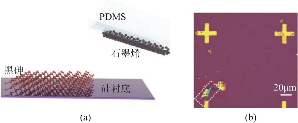
    Li-Bo ZHANG, Chuan-Sheng ZHANG, Lin WANG, Huai-Zhong XING. Broadband detector based on graphene-black arsenic heterostructure[J]. Journal of Infrared and Millimeter Waves, 2021, 40(6): 778
    Download Citation