
Dezhi Tan, Ke Sun, Zengling Li, Beibei Xu, Jianrong Qiu. Photo-processing of perovskites: current research status and challenges[J]. Opto-Electronic Science, 2022, 1(11): 220014
- Opto-Electronic Science
- Vol. 1, Issue 11, 220014 (2022)
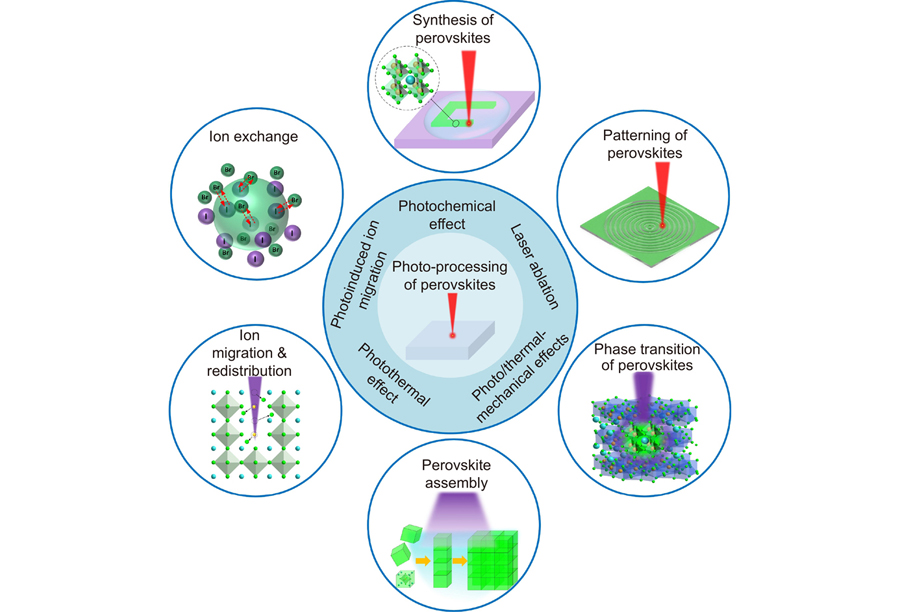
Fig. 1. Schematic overview of the current research on the photo-processing of perovskites.
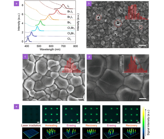
Fig. 2. (a ) Optical absorption spectra (dash curves) and PL spectra (solid curves) of CsPbX3 perovskite NCs with various halide compositions. SEM images of perovskite films produced by (b ) thermal annealing, (c ) nanosecond laser writing, and (d ) nanosecond laser writing with addition of carbon quantum dots. Scale bar, 500 nm. (e ) Optical images and PL mapping of a CsPbBr3 perovskite array during the erasing–recovery processes excited by UV light. Scale bars: 100 μm. Figure reproduced with permission from: (a) ref.43, Elsevier; (b–d) ref.69, John Wiley and Sons; ref.75, Springer Nature.
Fig. 3. (a ) Mechanism of UV light induced patterning of perovskite NCs. (b ) Patterning of various perovskite NCs. SEM images of the CsPbBr3 microlenses (c ) and surface gratings (d ). Figure reproduced with permission from: (a, b) ref.42, under a Creative Commons AttributionLicense 4.0; (c, d) ref.53, John Wiley and Sons.
Fig. 4. (a ) Schematic of ultrafast laser–induced liquid nanophase separation and generation of CsPb(Br1−xIx)3 perovskite NCs. (b ) PL mappings and spectra of CsPb(Br1−xIx)3 perovskite NCs. Scale bar: 10 μm. (c ) PL mappings and spectra of perovskite NCs in the Cl−-Br−-I− codoped glass. Figure reproduced with permission from ref.33, American Association for the Advancement of Science.
Fig. 5. (a ) Schematic diagram of laser induced phase transition from CsPb2Br5 to CsPbBr3 inside a CsPb2Br5 microplatelet. (b ) PL spectra of CsPbBr3 generated by laser irradiation with various times (65 s per time). (c ) The integral PL intensity as a function of the excitation intensity. (d ) Schematic diagram of the strong cavity mode spontaneous emission of the laser-written CsPbBr3 in the CsPb2Br5 microplatelet. Figure reproduced with permission from ref.97, American Chemical Society.
Fig. 6. (a –d ) Light induced shape evolution of CsPbBr3 nanostructures with an increase in irradiation. (e ) Schematic of light-induced ligand removal mechanism and assembly of CsPbBr3 nanocubes. (f ) High-angle annular dark-field scanning transmission electron microscopy image of assembled nanostructures. (g ) Cubic and (h ) spindle perovskite superlattices. Figure reproduced with permission from: ref.102, American Chemical Society; ref.105, John Wiley and Sons.
Fig. 7. (a ) SEM images of a CsPbBr3 nanowire with laser-patterned nanogratings. (b ) A schematically nanowire laser with vertically emitting light from its upper face. (c ) PL image of the nanowire laser. (d ) Photodetector arrays based on laser-written perovskites. Figure reproduced with permission from: (a−c) ref.51, American Chemical Society; ref.70, John Wiley and Sons.
Fig. 8. (a ) Schematic illustration of micro-LED devices with laser-written perovskite NCs inside a glass. (b ) A dynamic holographic display. (c ) PL mapping of the 3D perovskite dots in glass. (d ) PL mapping of a perovskite pattern with tunable emission wavelength. Figure reproduced with permission from ref.33, American Association for the Advancement of Science.


Set citation alerts for the article
Please enter your email address

© Copyright 2018-2021 | Chinese Laser Press. All Rights Reserved 沪ICP备15018463号-20