Abstract
The past two decades have seen a drastic progress in the development of semiconducting metal-halide perovskites (MHPs) from both the fundamentally scientific and technological points of view. The excellent optoelectronic properties and device performance make perovskites very attractive to the researchers in materials, physics, chemistry and so on. To fully explore the potential of perovskites in the applications, various techniques have been demonstrated to synthesize perovskites, modify their structures, and create patterns and devices. Among them, photo-processing has been revealed to be a facile and general technique to achieve these aims. In this review, we discuss the mechanisms of photo-processing of perovskites and summarize the recent progress in the photo-processing of perovskites for synthesis, patterning, ion exchange, phase transition, assembly, and ion migration and redistribution. The applications of photo-processed perovskites in photovoltaic devices, lasers, photodetectors, light-emitting diodes (LEDs), and optical data storage and encryption are also discussed. Finally, we provide an outlook on photo-processing of perovskites and propose the promising directions for future researches. This review is of significance to the researches and applications of perovskites and also to uncover new views on the light-matter interactions.The past two decades have seen a drastic progress in the development of semiconducting metal-halide perovskites (MHPs) from both the fundamentally scientific and technological points of view. The excellent optoelectronic properties and device performance make perovskites very attractive to the researchers in materials, physics, chemistry and so on. To fully explore the potential of perovskites in the applications, various techniques have been demonstrated to synthesize perovskites, modify their structures, and create patterns and devices. Among them, photo-processing has been revealed to be a facile and general technique to achieve these aims. In this review, we discuss the mechanisms of photo-processing of perovskites and summarize the recent progress in the photo-processing of perovskites for synthesis, patterning, ion exchange, phase transition, assembly, and ion migration and redistribution. The applications of photo-processed perovskites in photovoltaic devices, lasers, photodetectors, light-emitting diodes (LEDs), and optical data storage and encryption are also discussed. Finally, we provide an outlook on photo-processing of perovskites and propose the promising directions for future researches. This review is of significance to the researches and applications of perovskites and also to uncover new views on the light-matter interactions.Introduction
Metal-halide perovskites possess (MHPs) the general chemical formula of ABX3, where A is an alkali metal or organic cation (e.g., cesium (Cs+), methylammonium (MA+, CH3NH3+), or formamidinium (FA+, CH(NH2)2+)), B is a divalent metal cation of Pb2+ or Sn2+, and X− is a halide ion1. MHPs have emerged as a remarkably promising class of semiconducting materials due to the impressive optoelectronic properties, such as tunable bandgap, narrow emission, and high carrier mobility, which endow them with great potentials in diverse photovoltaic and optoelectronic applications2-7. For example, MHP devices for solar cells, LEDs, displays, X-ray scintillators and light communication have been demonstrated to show exceptional performance8-14. Until now, various techniques have been developed for perovskite processing as well as the device fabrication, such as colloid synthesis, mechanochemical synthesis, film processing, and mask-assisted patterning6, 10-12, 15-17.
Photo-processing has been established as a powerful technique for material synthesis, structure modification, and patterning in the semiconductor science and technology18-23. Compared to other common processing methods, photo-processing possesses several advantages, such as high area-selectivity, good compatibility with flexible substrates, and high scalability24, 25. More importantly, laser direct writing has been shown to be a facile mask-free lithography technique to create desirable and arbitrary patterns, which is crucial for fabrication of micro-optoelectronic devices26-31. As a result, photo-processing is frequently adopted in the perovskite research and applications32. Furthermore, the ions, typically the halide ions, exhibit high mobility due to the ionic crystal structure nature, which offers unique possibility for photo-processing of perovskites in the synthesis, structure modification and device fabrication33.
Photo-processing can induce various effects on the perovskites as well as the device performance34, 35. As a typical example, light irradiation can induce serious degradation of the perovskites, generation of defects and phase segregation in mixed-halide perovskites such as CsPbBr3–xIx, which lead to a decrease of the device performance and greatly hinder the application of perovskites36-40. On the contrary, light irradiation is also able to play a critical and “positive” role in the formation and patterning of perovskites, modifying the structures, tuning the optoelectronic properties and improving the device performance28, 41, 42. For example, light irradiation can induce generation of perovskites in solution, films and transparent solids, and also enable controlling ion distribution in the perovskites for tuning the bandgap33, 43.
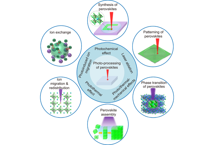
This review aims to provide a survey of the current status of the photo-processing of perovskites. We systematically summarize and discuss the mechanisms and progress in photo-processing of perovskites for synthesis, patterning, ion exchange, phase transition, assembly, and ion migration and redistribution (Fig. 1). The applications of the photo-processed perovskites are also discussed. Finally, we provide a brief outlook for the development and challenges to the photo-processing of perovskites.

Figure 1.Schematic overview of the current research on the photo-processing of perovskites.
Mechanisms about photo-processing of perovskites
Many reactions occur during the photo-processing of perovskites, which can originate from various mechanisms.
Photochemical effect
Light irradiation is able to trigger a series of chemical reaction between the precursors, and the perovskites and surfactants or surface ligands. In this case, chemical effect, but not the thermal effect, is crucial. For instance, the solar irradiation can induce crosslinking of benzyl acrylate molecules via the polymerization of acrylic group, which leads to formation of a compact and hydrophobic layer on the perovskite film surface44. The cross-linked interfacial layer can heal the interface defects of the perovskite films and also protect the device from water and oxygen. As a result, the efficiency and the stability of perovskite photovoltaic device are promoted. The light is also able to break the bonds of precursors and produce halide ions for the formation of perovskites43. The photoinduced modification of the surfactants also enables controlling the surface states of the perovskite nanocrystals (NCs), which is adopted to modulate the solubility of NCs in the solution for patterning45.
Photothermal effect
Generally, the local temperature increases significantly with an increase in the laser power or fluence, and the temperature change can reach hundreds of degrees Celsius, which is mainly attributed to the light absorption by the substrates, the precursors, and the perovskites46-49. The rate of temperature increase depends on laser wavelength, pulse repetition, the morphology of the perovskites (e.g., the films or NCs), and the bandgap of the perovskites. Suitable temperature and thermal field enable perovskite nucleation formation, crystal growth and annealing. Compared with the traditional homogeneous heating, light induced heating can be highly localized by modulating the focal positions and the spot size. Consequently, direct writing of desirable perovskite patterns with spatial selection is achievable in two-dimension and even three-dimension. This flexible designability allows for unique potential in the fabrication of micro-sized optoelectronic devices, such as micro-LEDs, photodetectors, lasers and memory devices.
Laser ablation
The thermal effect plays a critical role in the structure modifications of perovskites with continuous wave lasers or nanosecond lasers50. In another case, femtosecond laser allows for “cool” processing of the material surface, during which the thermal effect can be negligible, and is suitable for high-resolution patterning and ablating51-53. Femtosecond laser ablation is a complex process involving multiphoton absorption, photocarrier generation, thermalization, thermal diffusion, phase transitions and explosion, shock wave formation, and ultrafast cooling54. Laser alation is applicable to polishing the surface and patterning functional structures on the perovskite films and single crystals. For example, a femtosecond laser with an ultrashort pulse duration of 35 fs and a lower repetition rate of 1 kHz was adopted to polish the surface of perovskite films and a top layer with the thickness of 20 nm was removed55. The photoluminescence (PL) intensity of perovskites was enhanced significantly and this indicated that the density of the defects as well as the nonradiative recombination decreased after femtosecond laser polishing. Besides the laser irradiation parameters, such as wavelength, repetition rate, pulse duration and laser power density, the laser ablation is also dependent on the thermal conductivity and refractive index of perovskites. Small thermal conductivity is favorable for the high-resolution ablation and producing smooth structuring. The characteristic diameter (σ) of the energy deposition can be expressed as σ = [d2+(2kτ)2]1/2, where d is the focal spot size, k is the thermal conductivity and τ is the thermalization time53.
Photoinduced ion migration
Light illumination is able to create plenty of photocarriers, whose separation, accumulation and trapping by the defects lead to generation of an electrical field56, 57. Consequently, the mobile halide ions are driven by this established field and fill the defects, such as vacancies and interstitials. This ion migration may occur both in the horizon and vertical directions58. A reduction in traps and the subsequent non-irradiative recombination is expectable and this results in an enhancement in the PL. The trap annihilation rate increases with the light power density, the temperature and the activation energy of ion migration56. Typically, the activation energy for the I− migration is determined to be approximately 0.2 eV56, 59. In addition, photoinduced ion migration may also give rise to a notorious phenomenon: phase segregation, which seriously reduces the stability of the mixed-halide perovskite structures and devices60. Fortunately, the phase segregation can be reversed by light illumination with sufficient high intensity34.
Photo/thermal-mechanical effects
Besides the photochemical and photothermal effects, the photoinduced mechanical effect, such as strain, also provides an effective route to modify the properties of perovskites61-63. Femtosecond laser shocking was used to generate high pressure of up to 15 GPa on the surface of the 2D perovskite62. The shock pressure (P(τ)) can be determined by61: P(τ) = [(mαI0)/(2τ(α+1))]1/2, where m is the mass of the target layer, I0 is the laser power density, α is 0.1 and τ is the pulse duration. This technique enables tuning the bandgap of the perovskites and also reduces the residual tensile stress in the film. Pore-free perovskite thin films after femtosecond laser shock processing are obtainable, which can significantly improve the stability of the perovskite structures and devices. As a result, femtosecond laser shock processing allows for regulating the structure and properties of perovskites in a mechanical approach.
Photo-processing of perovskites
Photoinduced synthesis of perovskites
Photoinduced synthesis of perovskites mainly relies on two mechanisms: photochemical and photothermal effect. In the first case, photoirradiation is an effective and facile technique to control the concentration of components such as halide ions that form perovskites. For example, ultraviolet (UV) light irradiation can break the covalent carbon-halogen (C-X) bond of haloalkanes and produce halide ions for synthesis of perovskites43. Based on this principle, CsPbX3 NCs and nanocomposites (such as upconversion nanoparticles@mSiO2@CsPbX3 core/shell structures) were prepared in the solution, which open up new opportunities for multifunctional perovskite-based materials and devices for photonic applications. By controlling the concentration of haloalkanes, and the irradiation power and time, the bandgap of perovskites was tuned, as shown in Fig. 2(a).
Figure 2.(a) Optical absorption spectra (dash curves) and PL spectra (solid curves) of CsPbX3 perovskite NCs with various halide compositions. SEM images of perovskite films produced by (b) thermal annealing, (c) nanosecond laser writing, and (d) nanosecond laser writing with addition of carbon quantum dots. Scale bar, 500 nm. (e) Optical images and PL mapping of a CsPbBr3 perovskite array during the erasing–recovery processes excited by UV light. Scale bars: 100 μm. Figure reproduced with permission from: (a) ref.43, Elsevier; (b–d) ref.69, John Wiley and Sons; ref.75, Springer Nature.
The light beam can also act as a local heating source and increase the local temperature in the films, which enables fast growth and in situ patterning of perovskites. Absorption of laser energy by the substrates or the perovskite precursors is responsible for the local temperature increase. A continuous wave laser with the wavelength of 750 nm was used to directly write lead halide perovskite by Chou et al. without using a mask64. In this case, an absorbing substrate is usually necessary for efficient heating and temperate increase to generate crystal nucleation and induce crystal growth. Rapid crystallization of MAPbI3 perovskite films was also introduced by 450 nm, 532 nm and 1064 nm continuous wave lasers65-67. The morphology of the films was improved significantly to be homogeneous, dense and pinhole free, which enhanced the performance of the perovskite solar cells. The localized temperature gradient generated on the perovskite grain boundary was suggested to act as an effective driving force for the crystallization of the perovskite and the grain growth, which will enhance the light absorption and further increase the local temperature, leading to large sized perovskite grain. As a result, the average grain size of perovskites in the laser writing film can be much larger than that in the conventional thermal-annealing film, which was beneficial for charge transport from perovskite to charge collection layers as well as reducing the defects in the film. Consequently, the performance of the photovoltaic devices is improved significantly47. It is worth to note that the grain size and the crystal quality of the perovskites in the films can be tuned by controlling the laser power, wavelength and writing speed.
In situ photopatterning CsPbI3 perovskite NCs was also achieved by using pulsed lasers, such as 405 or 1064 nm nanosecond laser68, 69 and high repetition 800 nm femtosecond laser70, 71. The PL quantum yield reaches 92% and the obtained minimum line width is 0.9 μm68. Compared with the thermal annealing route, nanosecond laser can generate higher compacted perovskite films with larger crystal size (Fig. 2(b–c))69. The size further increases with the addition of carbon quantum dots in the perovskite film to be approximately 10 times larger than that by thermal annealing (Fig. 2(d)). The carbon quantum dots locating at the grain boundary of the perovskites can absorb laser energy significantly, which results in fusion of grain boundary, recrystallization and the growth of perovskite crystals. An 80 MHz femtosecond laser is also able to induce obvious local heating effect on the silicon substrate and promote nucleation and growth of MAPbI3 perovskite crystals in the liquid film70. Here, the size of the perovskite crystals is highly dependent on the laser power and can reach several micrometers.
Ultrafast laser induced thermal effect has been demonstrated to modulate the element distribution and local structure in the amorphous matrix such as glass72, 73. The highly nonlinear process during ultrafast laser-matter interaction provides unique capability for patterning functional structures at an arbitrary position in three-dimension. Relying on this principle, inorganic perovskite NCs (e.g., CsPbCl3, CsPbBr3 and CsPbI3) were written in the various glasses74-78. The glass matrix provides effective protection to keep NCs away from the environment. The emission can be tuned by controlling the irradiation parameters, such as pulse repetition rate, pulse duration, power and irradiation time, and the glass compositions. When the pulse repetition rate is low (e.g., 1 kHz), thermal annealing for several hours is necessary to create emissive perovskite NCs, which is time and energy consumption75, 76. When the repetition rate is high enough (e.g., 100 kHz), strong thermal accumulation will be generated and drive element re-distribution. Perovskites can be generated during the cooling process. However, the full width at half maximum (FWHM) of the PL spectrum is usually very large that indicates the presence of poor crystal structure74. As a result, thermal annealing is adopted to improve the crystal quality and emission properties of perovskites. Sun et al. reported that synergistically tuning the pulse duration, repletion rate and pulse energy, ultrafast laser can directly write high quality 3D CsPbCl3, CsPbBr3 and CsPbI3 perovskite NCs in the glass72. It is worth to note that the pulse duration is demonstrated to play a critical role in engineering of thermal accumulation. Generally, the pulse duration at around 1 picosecond is the most suitable parameter for writing highly emissive perovskite NCs, which confirmed that thermal effect is necessary for the formation of perovskite NCs. Furthermore, the perovskite NCs can be erased by irradiation of another ultrafast laser and are rewritable at the same position (Fig. 2(e)). Unfortunately, the PL of perovskites in the glass is generally tuned in a small range (< 50 nm) within one glass. In fact, continuously tailoring the PL of solids in a broad range from blue to red wavelength is nearly impossible using the conversional techniques.
Besides the above two principles, light activated nucleation was also observed41. In the sequential deposition for forming perovskite films, the PbI2 can absorb light to create electron-hole pairs, which enhances the nucleation rate and gives rise to a higher nucleation density. Consequently, generation of compact perovskite films with more homogeneous crystal size distribution was achieved. The perovskite photovoltaic devices fabricated under 1 sun irradiation show the power conversion efficiency (PCE) of 13.7%. For comparison, the PCF of the devices fabricated under the dark conditions is only half. This work opens up new an avenue to tune morphology of perovskite films and improve the device performance.
Photopatterning of perovskites
Photopatterning can be classified into two classes: ex situ and in situ patterning. The former one generally needs two steps including preparation of perovskites and patterning, which is discussed in this sub-section, and these two steps finish simultaneously in the latter one that is discussed in the previous sub-section.
Pan et al. reported photopatterning of the as-prepared CsPbX3 NCs by using a 405 nm lamp, which can induce cleavage of the photosensitive bound oxime sulfonate ester (PA-480)45. To this end, the photosensitizer firstly binds to the NCs and is cleaved at the N−O bond during photoirradiation, which causes a NC solubility variation in the solution such as toluene. After development, patterned films are achieved. The emission wavelength of the perovskite NCs is tunable across the visible region by the anion exchange. Recently, a modified technique with ligand cross-linkers (bisazides) is demonstrated42. The photoactive cross-linkers (e.g., singlet nitrene radicals) can be created under UV light illumination, which will covalently bond to the native, alkyl ligands that are adjacent NCs, as shown in Fig. 3(a). As a result, the solubility of NCs in the nonpolar solvents (e.g., toluene) decreases and cross-linked NC networks are formed. Consequently, uniform patterns can be produced and the resolution reaches the limit of the photomasks. Generally, this technique is applicable to all the CsPbX3 NCs, and even multicolored patterns (Fig. 3(b)). However, the performance of CsPbI3 NC patterns is not as good as that of CsPbCl3 and CsPbBr3 NC patterns, due to the intrinsic instability of CsPbI3 NCs. As a result, red-emitting NCs composed of II-VI compounds were adopted for the formation of RGB patterns. In addition, a mask is necessary for the patterning process with light emitting diodes (LEDs) or lamps, which is not friendly for designing arbitrarily shaped patterns.
Figure 3.(a) Mechanism of UV light induced patterning of perovskite NCs. (b) Patterning of various perovskite NCs. SEM images of the CsPbBr3 microlenses (c) and surface gratings (d). Figure reproduced with permission from: (a, b) ref.42, under a Creative Commons AttributionLicense 4.0; (c, d) ref.53, John Wiley and Sons.
Laser is also a powerful tool that enables high-resolution photopatterning of perovskite in the solid state such as films and single crystals by ablating and inducing ion exchange79-82. The intrinsic mask-free fabrication capability allows for writing arbitrarily shaped perovskite patterns for optoelectronic devices, such as irregularly shaped cavities79. A 405 nm continuous-wave laser was adopted to pattern perovskites, which relied on the laser induced removal of surfactant around the perovskite NCs83. In this regard, photoactive surfactant is necessary. The line width decreases with an increase in the laser scanning speed and a reduction in the laser power. The minimum linewidth is approximately 3.3 µm. In another case, the surface ligands bound to perovskite NCs can also be removed by the localized heating via irradiation of a 400 nm femtosecond laser and no photoactive ligands was used84. Sintering occurs subsequently and results in formation of perovskite patterning. To get final patterns, however, a washing process is needed to remove the perovskite NCs in the non-irradiated area. An incident femtosecond laser beams can induce decomposition of the mixed-halide perovskite (FAPb(BrxI1−x)3) nanoplatelets and redistribution of halide composition, through which the emission properties are spatially tunable80. Patterning of red, green and blue perovskite NCs was demonstrated by Liang et al. via femtosecond laser direct writing85. The minimum line width could reach 1.58 μm. The authors suggested that the Marangoni effect plays a critical role and induces a circulating flow, thereby pulling and accumulating the perovskite NCs to the bottom. After drying, the perovskite NCs were aggregated on the substrate along the laser scanning path and formed designed patterns.
A variety of structures were created by femtosecond laser irradiation on the surface of MAPbBr3 single crystals and PL enhancement was observed at the irradiated domain, which was suggested to originate from several factors, such as the photon recycling, light outcoupling and surface passivation86. Relying on the low thermal conductivity and high defect tolerance of perovskites, high-resolution patterning of halide MAPbI3 perovskites was revealed by Zhizhchenko et al. with a femtosecond laser81. They demonstrated that multi-pulse laser writing has the potential to ablate the perovskite more efficiently compared with the single-pulse, and allow for decreasing the size of the surrounding ablation area and precise thinning of halide perovskite film, which is critical for high resolution non-destructive patterning. Highly ordered MAPbI3 perovskite nanoholes and nanostripes with the width as small as 250 nm can be fabricated. Furthermore, ultra-smooth micro-optic elements (such as parabolic microlenses and truncated microaxicons, Fig. 3(c)) were directly written on the surface of CsPbI3 perovskite single crystal microplates and the feature size of structures was down to the deep subwavelength region (~λ/7, λ=515 nm: wavelength of femtosecond laser) with two-step processing, as shown in Fig. 3(d)53.
Besides laser ablation-based patterning, a 405 nm confocal continuous-wave (CW) laser was reported to create defective patterns on the CsPbBr3 micro-platelets87. It is interesting that the defective patterns are nearly invisible under optical microscopy without UV light irradiation, which promises the potential in the applications of micro-encryption and anticounterfeiting. As the PL of perovskite quenches significantly with temperature increase, laser induced photothermal effect was used to cause reversible PL quenching and create perovskite patterns88. To this end, perovskite NCs and CsYb2F7 NCs were produced inside the corresponding glass via heat-treatment to form perovskite@glass and CsYb2F7@glass. Then, these two glasses were grinded into powers and mixed together. The CsYb2F7 NCs in the glass can absorb photon energy from a 980 nm laser, increasing the local temperature up to 460 °C at the laser power of 2.2 W. As a result, when the mixed compositions were irradiated by a 980 nm laser and a 365 nm laser at the same time, the photothermal effect significantly quenched the PL of perovskite NCs excited at 365 nm. Therefore, the photothermal effect offers a reliable strategy to controlling the patterning information for anti-counterfeiting application.
Photoinduced ion exchange
The bandgap as well as the emission wavelength of perovskites is flexibly tunable by modulating halide compositions in the crystal lattice to cover the entire visible wavelength range, which also allows for improving the device stability6, 89. Consequently, ion exchange was developed to control the ratio of Cl/Br or Br/I in the perovskites and subsequently to engineer the bandgap and PL properties of perovskites. This compositional engineering is critical for fabricating high performance and stable perovskite devices90, 91. In this sub-section, we focus on the effect of tuning the bandgap of hybrid perovskites relying on ion exchange, one kind of photoinduced ion migration and redistribution.
To tune the halide composition and the bandgap of perovskites, a nanosecond laser with the wavelength of 532 nm or a coiled white LED strip has been adopted to induce ion exchange in solution92, 93. The halide ions can be released through laser induced photolysis of halocarbon solvent (e.g., CHCl3, CH3CH2I), breaking the C-X bonds. The subsequent ion exchange allows for tuning the bandgap of CsPbBr3 NCs with the emission range covering 410 to 650 nm by modulating laser irradiation time and power density92. Multicolor patterning was demonstrated by controlling the photoinduced ion exchange and using a light-source-integrated Dimatix inkjet printer with the diameter of pixel in the order of 50 μm93.
Continuous wave lasers have also been frequently adopted to modify the properties of perovskites or in situ generate perovskites in solution. For example, a 405 nm laser can induce photoelectrons in CsPbX3 NCs, which transfer to the dihalomethane molecules (e.g., dichloromethane and dibromomethane) and lead to subsequent reductive dissociation of solvent molecules94. As a result, halide ions can be generated for anion exchange along with tuned bandgap and PL.
Ion exchange is usually carried out in solution to modify the halide composition in perovskites. How about in the solids? Sun et al. reported a unique strategy for engineering the chemical composition and then the bandgap of perovskite NCs in the glass by using in situ 3D ultrafast laser direct writing33. The authors proposed that liquid perovskite domains consisted with elements for formation of perovskite NCs can be generated via ultrafast laser induced liquid nanophase separation. The halide ion distribution was modulated at the nanoscale by tailoring the local temperature and pressure via controlling the pulse repetition rate, pulse duration and power. In this case, the behavior of ions, such as the diffusion rate and direction, was determined by the local conditions, the complexation of Pb2+-halide ions, and the radius and weight of halide ions. By taking Br−-I− doped glass as an example, Br− ions diffuse faster into the liquid perovskite regions than I− ions do owing to the larger complexation of Pb2+-Br−, lighter weight, and smaller radius of Br− ions, forming Br−-rich liquid perovskite. Furthermore, during the continuous laser illumination, the halide ion exchange (e.g., exchange between Br− ions in liquid perovskites and I− ions in liquid glass) happens due to the chemical potential gradient, which enables dynamically tuning the concentration of the halide ions in the liquid perovskite domains, as shown in Fig. 4(a). As a result, the PL of the perovskite NCs was continuously tuned from 520 nm to 690 nm, indicating the transformation of CsPbBr3 into CsPbI3 NCs. This technique was proved to be general to write composition and bandgap tunable perovskite NCs in the Cl−-Br−, Br−-I− (Fig. 4(b)) and Cl− -Br− -I− codoped glasses (Fig. 4(c)). Typically, transforming CsPb(Cl1-xBrx)3 into CsPb(Br1-xIx)3 and further into CsPbI3 perovskites was achieved by controlling the laser parameters and irradiation time. Consequently, the PL of perovskite NCs was tailored in a broad range from blue to red. Perovskite NCs usually exhibit poor stability due to chemical- and thermal-induced decomposition, and light-induced phase segregation. The perovskite NCs produced in the glass show excellent stability when exposed to ultraviolet irradiation (power density up to 32 W/cm2), organic solution (e.g., ethanol), and high temperatures (up to 250 °C). No degradation or phase separation was observed during the testing time.
Figure 4.(a) Schematic of ultrafast laser–induced liquid nanophase separation and generation of CsPb(Br1−xIx)3 perovskite NCs. (b) PL mappings and spectra of CsPb(Br1−xIx)3 perovskite NCs. Scale bar: 10 μm. (c) PL mappings and spectra of perovskite NCs in the Cl−-Br−-I− codoped glass. Figure reproduced with permission from ref.33, American Association for the Advancement of Science.
In addition, ion exchange in the liquid film can be expected when it is irradiated by lasers, which would be similar to that in solution. Light induced ion exchange may also occur in the perovskite film and perovskite/polymer composite film, which is dependent on the chemical compositions of the film and laser writing conditions. In this case, light can be used to control the release of the halide ions as well as the concentration by breaking the C-X bonds in the polymer, similar to the case in solution. Furthermore, ion exchange in perovskite film has been reported by putting the perovskite film in solution, which provides an easy way to locally modulate the bandgap and PL of the perovskite film92. Light induced ion exchange in the film would be an interesting topic for the future work by optimizing the precursors and parameters, and is important for modifying the optical properties of perovskites on flexible substrates.
Photoinduced phase transition of perovskites
Perovskites can exhibit several phase structures, which may be luminescent or non-luminescent. Photo-processing enables triggering and controlling the phase transition behavior. Zou et al. demonstrated that laser induced thermal effect caused phase transition from orthorhombic (δ) phase (non-perovskite phase) to cubic (α) phase (perovskite phase)95. A relatively low laser power of 9 mW with the wavelength of 1064 nm allows for a temperature rise of 160 °C in the focused domain through the absorption of silver or indium tin oxide film, which is high enough for phase transition in 10 min. It is worth to note that this phase transition is reversible by exposing the perovskite to moisture for 30 min. As a result, nonvolatile rewritable photomemory arrays were fabricated for optical data storage based on this reversible phase-change of perovskites. A continuous-wave laser with short wavelength of 458 nm can directly trigger phase transition from δ-phase of FAPbI3 into its luminescent black α-phase without using the light absorption layer96. In this case, in situ Raman spectroscopy showed that nearly 100 min was needed for completing the phase transition with the laser power density of 500 W/cm2. Steele et al. conformed the atmospheric conditions such as the presence of the oxygen strongly influence the phase transition behavior96. For example, the oxygens may intercalate into the perovskite crystal lattices, forming Pb-O bonds, which is possible to decrease the energy barrier for phase transition and facilitate this transition.
Besides the inorganic-organic hybrid perovskites, a suitable laser enables inducing phase transition of all inorganic perovskites due to the elevated local temperature, which may be accompanied with the modification of chemical composition. A 325 nm continuous-wave laser was reported to initiate phase transition from CsPb2Br5 to CsPbBr3 in the CsPb2Br5 microplatelets (Fig. 5(a)) and the generated CsPbBr3 exhibit quantum confinement effect97. It is interesting that the PL of these written CsPbBr3 has a series of sharp emission lines (Fig. 5(b)) and the PL intensity (I(p)) shows a superlinear excitation power dependence (p) as I(p) ∞ p2 83, which originates from the cavity resonance (Fig. 5(c)). A Fabry-Perot microcavity was formed with the upper and lower surface of the CsPbBr3 microplatelet acting as mirrors (Fig. 5(d)). In comparison to the free space case, the Purcell effect leads to enhancement of the quantum transition rate by 2 orders of magnitude. Due to the protection of the CsPb2Br5, the stability of CsPbBr3 is improved significantly. This work indicates that CsPbBr3 written by laser holds great potential in the applications of low-threshold lasers and information encryption.
Figure 5.(a) Schematic diagram of laser induced phase transition from CsPb2Br5 to CsPbBr3 inside a CsPb2Br5 microplatelet. (b) PL spectra of CsPbBr3 generated by laser irradiation with various times (65 s per time). (c) The integral PL intensity as a function of the excitation intensity. (d) Schematic diagram of the strong cavity mode spontaneous emission of the laser-written CsPbBr3 in the CsPb2Br5 microplatelet. Figure reproduced with permission from ref.97, American Chemical Society.
An ultrafast laser is also promising to induce phase transition, which is able to write 3D emissive perovskite in the transparent solids such as transparent non-perovskites bulks and non-perovskite-polymer composites by controlling the phase transition. For example, Li et al. reported writing of CsPbBr3 in CsPb2Br5 single crystals with a femtosecond laser98.
Photoinduced assembly of perovskite nanostructures
Photo-processing is a facile technique to modify the morphology of the perovskite nanostructures via assembly, which allows for modulating the optical properties and results in novel functional structures, such as superlattices99. For example, few-layered CsPbBr3 nanoplatelets were reported to be assembled into bulk phase with lamellar stacking when excited by a 325 nm laser100. The PL peak was observed to redshift from 436 nm to 466, 484, and 521 nm with increase of the irradiation time, and the emissions can be assigned to the 3-layer, 6-layer, 9-layer and bulk phase perovskites, respectively. A very low excitation intensity of 20 mW/cm2 is enough to trigger this assembly. In addition, the light illumination is also beneficial for the removement of the surface ligands, contributing to the assembly of perovskite nanoplatelets. However, one order of magnitude higher of the excitation intensity (500 mW/cm2) is necessary for assembly of CsPbBr3 nanocubes and the assembly of the lamellar stacking is even not applicable for the MAPbBr3 NCs. A LED at 365 nm with the power density of 200 mW/cm2 was also reported to induce assembly of the CsPbBr3 nanoplatelets into nanobelts with obvious PL redshift and enhancement101. It is interesting that moisture and/or oxygen are crucial to trigger this assembly behavior, whose mechanism is still unclear.
Light from a solar simulator with the power density of 170 mW/cm2 was demonstrated to initiate the assembly of CsPbBr3 nanocubes into nanowires (Fig. 6(a, d))102. In this case, the surface ligands (oleylamine) are removed owing to the light illumination (Fig. 6(e)). Oriented attachment and merging occur along the (110) direction (Fig. 6(f)), leading to assembly of CsPbBr3 nanocubes and growth in one dimension. The PL carrier lifetime of nanowires is about 125 ns and two orders of magnitude larger than that of NCs, which is assigned to the highly crystalline feature of CsPbBr3 nanowires with a long carrier diffusion length. Assembly along the (100) direction was also demonstrated to produce one-dimensional structure with the oleylamine as the surface ligand103. Furthermore, assembly of CsPbI3 nanocubes in two-dimension was realized relying on the light-driven oriented attachment104. Three-dimensional superlattices were formed via assembly of CsPbBr3 NCs induced by 360-nm-UV light (170 mW/cm2) and an over 1000-fold PL enhancement was observed105. Morphology is tunable by varying the carbon chain length of the surface-bound ligand molecule, 1-alkynyl acid. For instance, cubic (Fig. 6(g)) and spindle perovskite superlattices (Fig. 6(h)) were produced by using the 10-undecynoic acid (UDA) and 5-hexynoic acid (HA) as the protecting ligand, respectively.
Figure 6.(a–d) Light induced shape evolution of CsPbBr3 nanostructures with an increase in irradiation. (e) Schematic of light-induced ligand removal mechanism and assembly of CsPbBr3 nanocubes. (f) High-angle annular dark-field scanning transmission electron microscopy image of assembled nanostructures. (g) Cubic and (h) spindle perovskite superlattices. Figure reproduced with permission from: ref.102, American Chemical Society; ref.105, John Wiley and Sons.
Photoinduced assembly of perovskite nanostructures offers a new avenue to reveal the light-perovskite interaction and control the optoelectronic properties, which will be useful for constructing new perovskite structures and devices with unprecedented photonic and optoelectronic functionalities. However, until now, assembly has mainly been achieved for CsPbBr3 nanostructures and the mechanisms have not been fully uncovered.
Photoinduced ion migration and redistribution in perovskites
Due to the low activation energy for ion migration and the ionic nature of the perovskite, halide ions are highly mobile, which makes contribution to many photoinduced phenomena in perovskites, such as light soaking effect and significantly influences the performance of perovskite photovoltaic devices106.
Laser irradiation can induce obvious halide redistribution in organic–inorganic perovskite films, which allows for one order of magnitude reduction in trap state density via the halide filling the trap states. Both the PL lifetime and the intensity increase56, 107. Light from the solar simulator (1 sun) is also effective to induce obvious halide migration and passivate the defects, which boosts the PCE of the perovskite photovoltaic devices108, 109. Further investigations show that an increase in the built-in electric field can be generated under continuous light irradiation, which leads to an enhancement of the charge extraction ability and eliminates the interface recombination in the perovskite solar cells109, 110. Tsai et al. reported that lattice expansion can be generated by continuous light illumination in the FA0.7MA0.25Cs0.05PbI3 perovskite thin films and a significant enhancement in the PCE from 18.5 to 20.5% was obtained without compromising the device stability111. The authors suggested that the relaxation of local lattice strain induced by lattice expansion is responsible for the performance improvement with larger open circuit voltage and fill factor. However, the intrinsic mechanism of this light soaking effect is still under debate112. Although the light induced thermal effect may also cause lattice expansion, the heating alone cannot lead to enhancement of the PCE108, 109. The light soaking effect can be tuned by controlling the Br/I ratio in the CsPb(Br1−xIx)3 film and the device curing time for inducing maximum efficiency enhancement decreases with an increase in the Br/I ratio108. By introducing Cs+ in the FAxMA1-xPbI3 film, the halide migration can be suppressed and the accumulation of the mobile ions decreases, which gives rise to an increase in the PCE from 18.7% to 22.4%109.
In the quasi-2D perovskite photovoltaic devices, photo-carriers generated by light irradiation give rise to quasi-Fermi level splitting, which can induce favorable ion (e.g., I−) accumulation toward the anode113. Consequently, an electric field parallel with the built-in potential is generated and allows for significant improvement in the device performance with PCE increasing from 14.61% to 19.05%. This light induced ion accumulation enables long-term operation of perovskite devices.
Photoinduced ion migration and redistribution in the mixed halide perovskites can lead to obvious phase segregation with formation of various perovskite phases in different domains (e.g., Br-rich and I-rich phases in the CsPbBr1-xIx perovskites)106. Photoinduced phase segregation of perovskites generally possesses a serious issue on the stability of the device performance, which is not so easy to overcome by the traditional techniques, such as passivation and encapsulation. Recently, photoinduced remixing of halide ions in the mixed perovskites has been observed when exposed to light with high power density34. As a result, the phase segregation can be manipulated by controlling the light density, which enables writing-reading-erasing the designed patterns in the perovskites and holds potential in applications of optical data storage. In addition, a two-step illumination technique was developed to exploit the potential of phase segregation in the applications of opto-electronics57. Firstly, a 405 nm laser with the power density of 1500 W/cm2 was used to produce defect patterns with plenty of defect states in CsPb(Cl1−xBrx)3 perovskite microplatelets. Then, phase separation was induced by a wide light field with the power density of 550 W/cm2 and the directional halide migration results in the accumulation of Br- in the defective pattern, which exhibits green emission when excited by a 405 nm laser (50 W/cm2).
Photoinduced other modifications of perovskites
Perovskites easily degrade when exposed to light irradiation, which depends on the light power density, temperature, composition of perovskites, and light wavelength114-116. Photoinduced degradation is usually not good for the device performance, and limits the operation lifetime of perovskite devices117. For example, Barbe et al. reported that MAPbI3 decomposed to generate PbI2 during laser illumination, which has significant influence on the optical properties of perovskites and the device performance118. By varying the laser power and irradiation time, the laser decomposition process can be modulated that is able to control the thickness of PbI2 layer. When the thickness of the PbI2 layer is larger than 20 nm, an obvious detrimental effect was observed on the PL and photocurrent. However, under specific “mild” irradiation conditions, a thin PbI2 surface layer with the thickness of < 20 nm can be created that passivates the non-radiative defects and reduces the charge recombination at the interface, and finally causes a significant increase in the PL and photocurrent.
Structural fluctuations such as morphology/structural disorder and film heterogeneity in the organic–inorganic hybrid MAPbI3 perovskite films are easily generated during film processing, which are detrimental to the device performance. Instead of promoting degradation, a nanosecond pulsed UV laser was used to irradiate the perovskite thin films and led to rapid structure reconstruction with reduction of randomness in the morphology, disorder and heterogeneity, which reduces the density of recombination and extends PL lifetime of photocarriers and charge carrier mobility119. Similarly, illumination with a 248 nm KrF excimer laser is also able to delete the surface trap states, suppress the nonradiative recombination in the MAPbI3 perovskite films and finally improve PCE of the perovskite solar cells120.
As the perovskite NCs are an effective photocatalyst to trigger the photoinduced electron-transfer and the resultant polymerization121, controlled radical photocatalyzed polymerization has been reported for growing protective polymer brushes around the surface of the CsPbBr3 perovskite NCs themselves, forming CsPbBr3−polymer core-shell nanostructures122. Due to the protection of effect of the polymer, the colloidal stability and optical stability of the perovskite NCs are much improved when exposed to various polar organic solvents, water, and UV irradiation conditions.
In the femtosecond laser shock processing, the local pressure can increase from 0 to 15.45 GPa, which enables modifying the band structure of perovskites62. The bandgap decreases by 150 meV with the pressure of up to 2.75 GPa and FWHM of the PL spectrum increases with the shock pressure. The authors proposed that the bandgap modulation originated from the distortion of the inorganic frameworks (e.g., reduction of the unit cell lattice constants and bond length) and the broadening of FWHM originated from the weakening of the long-range order of the perovskite structures.
Applications of photo-processed perovskites
Photovoltaic devices
One of the most exciting motivations for the research on the perovskites is the impressive high PCE of the photovoltaic devices, reaching higher than 25% now123-125. Photo-processing is a promising technique for modifying the structures of the perovskites, and reducing the defects and non-radiative recombination, which can contribute to an increase in the PCE of the photovoltaic devices and enhancement of the stability55. For example, laser processing can decrease the density of the grain boundary and increase the size of perovskite grain (Fig. 2(c)). The fabricated perovskite devices exhibited an enhanced PCE, reaching 20.8%47, 55. Using the laser synthesized perovskites, photovoltaic devices were also fabricated with the PCE of up to 20% and a high open-circuit voltage of 1.146 V was achieved44, 126.
Lasers
Laser direct writing enables high resolution patterning of perovskite functional structures for photonics with flexible morphology designability in diverse perovskites such as films and nanowires79. For example, perovskite microdisks and nanowires can be fabricated by femtosecond laser ablation of perovskite film81, 127, 128. The diameter of the microdisks or the width and length of the nanowires are tunable. Single-mode lasing was observed at room temperature with the central emission wavelength at around 780–790 nm. The FWHM is less than 0.2 nm, the Q-factor reaches 5500, and the minimum lasing thresholds are as low as 150 and 7 μJ/cm2 for the nanosecond and femtosecond laser excitation, respectively. In another case, halide perovskite nanowires with nanogratings (Fig. 7(a)) on the surface show excellent directional lasing at around 541 nm, which can emit vertically from the nanowires (Fig. 7(b, c))51. The minimum FWHM is about 0.08 nm and the Q-factor is up to 6000.
Figure 7.(a) SEM images of a CsPbBr3 nanowire with laser-patterned nanogratings. (b) A schematically nanowire laser with vertically emitting light from its upper face. (c) PL image of the nanowire laser. (d) Photodetector arrays based on laser-written perovskites. Figure reproduced with permission from: (a−c) ref.51, American Chemical Society; ref.70, John Wiley and Sons.
Photodetectors
Perovskites produced by photo-processing, especially by laser direct writing show great advantages in fabricating micro-sized optoelectronic devices, such photodetectors, LEDs and displays, as it is very easy to create high-resolution patterns with the single unit size down to several micrometers. For example, Arciniegas et al. reported writing perovskites between the as-prepared electrodes with well controlling over the position and size of the perovskite structures (Fig. 7(d))70. This device exhibits good photoresponse in a wide wavelength range from 310 to 560 nm and the maximum responsivity reaches 0.83 A/W in the detecting range of 400–500 nm. Photodetectors were also fabricated by using photoinduced phase transition of perovskites95. The leakage current can reach as low as 10−8 A, which is critical for detecting weak light signal92. The flexible patterning capability endows the laser-written photodetector arrays with great potential in the applications of sensor chips, and displays64.
LEDs
The UV light illumination was demonstrated to increase the stability of CsPbBr3 perovskites even if exposed to various solvents, which is favorable for all-solution processed devices101. As a result, solution-processed green-emitting LEDs were fabricated and a peak external quantum efficiency (EQE) of 1.1% was obtained with a luminance of 590 cd/m2. The LEDs based on FAPbBr3 NCs show a peak EQE of 6.8% and the maximum luminance reaches 4700 cd/m2 42. Recently, micro-LEDs have been demonstrated by assembling a blue LED chip and laser-written dots in the glass (Fig. 8(a))33. In this case, glass acts as a key emissive component, not as a substrate any more. The smallest pixel size is about 6 μm, which allows for applications in high resolution displays. Furthermore, the 3D emissive perovskites in the glass can also be excited by holographic light. Consequently, dynamical holographic displays (Fig. 8(b)) and 3D displays were achieved.
Figure 8.(a) Schematic illustration of micro-LED devices with laser-written perovskite NCs inside a glass. (b) A dynamic holographic display. (c) PL mapping of the 3D perovskite dots in glass. (d) PL mapping of a perovskite pattern with tunable emission wavelength. Figure reproduced with permission from ref.33, American Association for the Advancement of Science.
Optical storage and encryption
As aforementioned, photo-processing, typically the laser direct writing, allows for creating the perovskite patterns with the dot size down to several micrometers, which hold great potential in the applications of optical storage and encryption42, 45, 68, 83, 95, 129. Especially, 3D (X, Y, Z position in space) optical storage is possible based on ultrafast laser direct writing in the glass33, 75, 76, 130. Hereby, ultrafast laser is focused in the glass and directly writes perovskite NCs at the desirable position (Fig. 8(c)), which enables flexible patterning. Furthermore, relying on the tunable emission behavior, a fourth-dimension with the varied emission wavelength is also available (Fig. 8(d))33. An increase in the dimension can contribute to increasing the capacity of the storage media. In addition, the written perovskite NCs can be erased and rewritten by the ultrafast laser beam, which is also meaningful for the actual applications of the perovskites in the optical storage and encryption72. Due to the protection of the glass matrix, long term optical storage with the perovskite NCs in glass is expectable131.
Challenges and outlooks
Photo-processing has been established a powerful technique for synthesis and structure modification of perovskites. In this work, we reviewed the progress of photo-processing of perovskites including the mechanisms, phenomena and applications. Although many efforts have been made to the research on photo-processing of perovskites and novel applications, there are still many challenges on the road to unravel the procedure and mechanism of photo-processing of perovskites, and explore more applications. 1) The dynamics of the photo-processing of perovskites is far from being fully understood132, 133. Techniques such as ultrafast electronic diffraction, time-resolved X-ray diffraction and photoemission electron microscopy (PEEM) should be useful to probe and detect the light induced structure evolution35, 132. Simulation will be also useful for understanding the mechanism of photo-processing of perovskites134. 2) How do molecules such as water and oxygen affect the photo-processing procedure? In most of the cases, photo-processing is performed under the atmospheric conditions and polar molecules inevitably influence the interaction between light and perovskites, typically accelerating the photo-processing, which is usually not under considered39, 96, 116, 135. 3) As the bandgap, stability and device performance of perovskites have been affected significantly by doping19. However, there has been no report about photoinduced doping in the perovskites, which will be an interesting research topic to study. 4) Although the photo-processing has endowed new functionalities with perovskites, many work focused one or several kinds of perovskites, mostly APbBr3 perovskites. Are the principles general to perovskites with other compositions, such as Pb-free perovskites and mixed halide perovskites? More investigations are needed to prove the generality of the demonstrated photo-processing routes for perovskites with various compositions. 5) There are usually inhomogeneity, defects, and grain boundary in the perovskites, especially in the films35. How do they influence the photo-processing dynamics? 6) Photo-processing can work for flexible substrates or perovskite films, which will be critical to the applications of perovskites in wearable electronics and optoelectronics. However, there are few reports to fully explore photo-processing of perovskites in flexible perovskites. 7) For the optical storage, display and photodetector applications, the dot size is still too large (typically larger than several micrometers). Decreasing the dot size is necessary for high-capacity data storage, high-resolution display and highly sensitive photodetectors in the future136. The dot size is generally determined by the thermal diffusion and diffraction limit. Decreasing the thermal effect, such as using femtosecond laser “cooling” ablation, will be helpful to create smaller perovskite dots137. Sub-diffraction lithography would be achievable to produce sub-micrometer dots by using two-beam writing, where one beam initiates the patterning and another (doughnut shape) beam inhibits the photochemical reaction138, 139.
In conclusion, significant challenges still remain in understanding the mechanisms of photo-processing. A more explorative direction for modulating the opto-electronic properties of the perovskite via photo-processing is expected. Besides, developing diverse optoelectronic devices based on photo-processed perovskites for the applications in optics and photonics is promising140, 141. Furthermore, the typical principles of the photo-processing techniques such as photochemical effect, photothermal effect, and laser ablation can be applicable to other NCs or quantum dots, such as CdTe, CdSe, InP, ZrO2, Fe2O3, Al2O3, and Au, with controlled light source and precursors18, 142-145. As a result, the discussions in this work will be generally important for photo-processing of various NCs or quantum dots.
Acknowledgements
We are grateful for financial supports from the National Key R&D Program of China (No. 2021YFB2800500), the National Natural Science Foundation of China (Grant Nos. U20A20211, 51902286), and Key Research Project of Zhejiang Lab.
The authors declare no competing financial interests.
References
[16] Zhou Y, Wang Y. Perovskite Quantum Dots: Synthesis, Properties and Applications (Springer, Singapore, 2020).
[123] The National Renewable Energy Laboratory, Best Research-Cell Efficiency Chart.https://www.nrel.gov/pv/cell-efficiency.html.