Abstract
We present a method to generate a frequency-doubled microwave signal by employing a coupling-modulated ring resonator. Critical coupling is achieved when the resonator intrinsic loss is perfectly balanced by the external coupling enabled by a Mach–Zehnder interferometer coupler. The high suppression of the carrier leads to a clean two-tone optical signal with the frequency interval two times larger than that of the input microwave frequency. The beating of the two-tone signal at a photodiode generates the frequency upconverted microwave signal. A theoretical model is established to analyze the modulation process and the microwave signal generation. Experimental results show that the electrical harmonic suppression ratio is around ~20 dB (29 dB) for an input microwave signal with 5 dBm (10 dBm) power.1. INTRODUCTION
Microwave photonics (MWP), the study of the interaction of microwave and optical signals, has been a hot research area recently [1,2]. MWP systems combine the advantages of microwave engineering and optoelectronics, but they are subjected to complex system configurations composed of discrete bulky optical and electrical components, which are power hungry, expensive, and unstable. The major functions in an MWP system include microwave signal generation, processing, and transmission in the optical domain.
In up-to-date microwave systems, the generation of a low-phase noise and frequency-tunable microwave is still a challenging task [3]. Traditionally, a microwave signal is generated by an electrical oscillator based on two terminal (diodes) or three terminal (transistors) devices. To obtain high-frequency microwave or submillimeter waves, the above approach of using many stages of frequency multipliers is still problematic because of the electrical bandwidth bottleneck and the lack of frequency tuning flexibility.
On the other hand, microwave signal generation in the optical domain has many merits, such as high bandwidth, light weight, low cost, etc. Various approaches can be used to generate the microwave signal in the optical domain, such as heterodyning two optical signals in a nonlinear optical crystal or a photodetector (PD) [4,5], using an opto-electronic oscillator [6,7] or a mode-locked laser [8,9]. Moreover, a high-frequency new microwave signal can be generated by modulating a high-speed optical modulator with a low-frequency microwave signal. Double or quadruple frequency generation in the optical domain using a commercial external modulator has been reported [10–13]. The method is quite attractive because of its system simplicity, operation stability, and good coherence of the two optical sidebands [14]. O’Reilly et al. first proposed to use a single commercial Mach–Zehnder modulator (MZM) in 1992 [15]. By adjusting the DC bias voltage to set the MZM at the minimum transmission point, all even-order sidebands can be eliminated, and a frequency-doubled microwave signal is obtained by beating st order sidebands at a PD. When the MZM is biased at the maximum transmission point, then the frequency quadrupling can be obtained by incorporating an imbalanced Mach–Zehnder (MZ) filter after the modulator [16]. The frequency of the generated microwave signal is limited by the fixed free spectral range (FSR) of the MZ filter. Qi et al. proposed an approach to utilize a narrow-bandwidth fiber Bragg grating (FBG) filter to suppress the unwanted carrier [13]. It is of critical importance to suppress the carrier no matter in double- or quadruple-frequency generation in order to obtain a high-quality microwave signal.
Sign up for Photonics Research TOC. Get the latest issue of Photonics Research delivered right to you!Sign up now
The above-mentioned optical techniques for microwave signal generation all use discrete components. Silicon photonics has been developed rapidly in recent years [17], which gives a low-cost, compact, and integration solution to MWP. It has the potential for monolithic integration of optical and electrical components on the same chip using the state-of-the-art CMOS facilities [18,19]. In 2015, Shao et al. demonstrated a method to generate a frequency-doubled microwave signal by using an on-chip silicon microring modulator [20]. The modulation bandwidth is ultimately limited by the cavity lifetime, which leads to a low conversion efficiency at a high microwave frequency. Moreover, the cavity intrinsic loss and external coupling coefficient are both fixed, which cannot guarantee a large resonance extinction ratio (ER) and high suppression of the carrier due to the fabrication imperfections and uncertainties.
In this paper, we demonstrate the microwave signal generation by using our previously demonstrated coupling-modulated ring resonator [21,22]. The key advantage of such a device for microwave frequency doubling is that the resonator coupling coefficient with the bus waveguide is tunable and thus the critical coupling is always attainable, leading to a high suppression of the optical carrier. Besides, as modulation is performed to the coupler and not directly to the cavity, the modulation bandwidth is not limited by the cavity lifetime [23,24], allowing for high-frequency microwave generation. A theoretical model for the coupling-modulated silicon ring resonator is established. Frequency-doubled microwave signal with a high suppression ratio (SR) between the first- and second- harmonic components is observed when the resonator approaches the critical coupling. The measurement results overall agree well with the predictions by the model.
2. DEVICE STRUCTURE AND WORKING PRINCIPLE
Figure 1(a) depicts the schematic structure of a coupling-modulated silicon ring resonator. The ring resonator consists of a Mach–Zehnder interferometer (MZI) with one output port routed back to form a resonance loop. The length difference of the two MZI arms is 10 μm, and the active arm length is 800 μm. The PN junctions are embedded in two MZI arms, and the traveling wave electrode (TWE) is used to make the modulator operate at the push–pull scheme. The microwave signal combined with a DC bias voltage via an external 65 GHz bias-tee is applied to the signal (S) and ground (G) metal lines through a 40 GHz microwave probe. In order to set the PN junctions to the carrier-depletion mode, another DC voltage is applied to the region through a DC electrode. and can be independently adjusted to freely set the coupling condition (under-coupling, critical or over-coupling) for each resonance. The inset illustrates the cross-section of the PN junction. The rib waveguide has a width of 500 nm, a height of 220 nm, and a slab height of 90 nm. The heavily doped regions are connected to the metal electrodes. The doping concentrations are and for the P- and N-doped regions, respectively. The PN junction has an offset of 100 nm toward the N-doping side. Light is coupled into and out of the device though two grating couplers with loss in total.
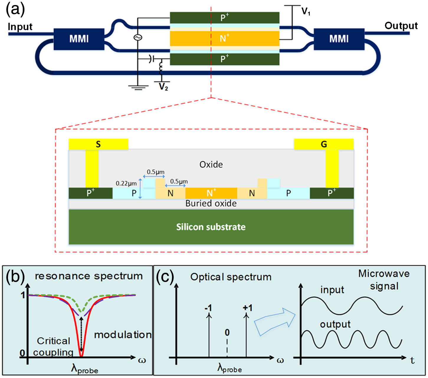
Figure 1.(a) Schematic structure of the coupling-modulated silicon ring resonator. Inset depicts the cross-sectional view of rib waveguides. (b) Resonance ER change upon modulation. (c) A frequency-doubled microwave signal is generated by beating the st-order sidebands at a PD.
For a single bus waveguide-coupled microring resonator [25], the coupling condition is pre-determined by the relative value of the resonator intrinsic loss and the coupling coefficient. It is difficult to change the coupling condition once the resonator is fabricated. Especially, when the resonance -factor is large, a small variation in the resonator intrinsic loss due to fabrication uncertainty may cause a significant change in resonance ER from the designed one.
In our design, the fixed coupler is replaced by a tunable MZI coupler so that the coupling coefficient can be conveniently tuned. The critical coupling condition can always be attained no matter what the initial condition is, which alleviates the stringent requirement for precise coupler design and cavity loss control. The critical coupling condition ensures a large ER, which is highly desired to suppress the carrier in the microwave upconversion process as will be elaborated on later.
Figure 1(b) shows the resonance spectrum evolution upon modulation. With the push–pull modulation of the MZI coupler, the resonance ER varies while the resonance wavelength is fixed. The modulation results in two-tone frequency components in the optical spectrum, and the beating of them in the PD generates the frequency-doubled microwave signal, as illustrated in Fig. 1(c). It should be noted that the optical carrier can be completely eliminated by setting the modulator to the null transmission wavelength with critical coupling.
3. THEORETICAL MODEL
The transfer matrix of the MZI coupler is given by where represents the optical field transmission in the MZI arms, and represent the phases in the top and bottom arms, respectively. We assume the phase difference of the two arms is in the range of [0, ], which covers the full tuning range of the MZI coupler. Then we have
The entire microring resonator can be modelled using the following two equations: where and (, 2) are the electric fields before and after the MZI coupler, respectively, represents the optical field transmission in the ring feedback waveguide, and is corresponding phase change.
From Eqs. (1)–(6), we obtain the input-normalized output field transmission as
When the round-trip phase change is ( is an integer), the resonance condition is satisfied, and we have
On resonance, the normalized output optical power is given by
The critical coupling requires zero transmission, leading to the following condition
In the silicon waveguide, the refractive index is changed based on the free-carrier plasma dispersion effect. The dependence of the effective refractive index of the waveguide on the applied voltage can be described by the polynomial expansion where is the drive voltage. The phases of the two MZI arms can be expressed as where is the phase difference due to the longer length of the top arm relative to the bottom arm.
In the static state, and are applied to tune the device to reach the critical point. Substitute Eqs. (12) and (13) into Eq. (2) and take into consideration the critical coupling condition in Eq. (10) and then the two DC bias voltages should satisfy
In the push–pull microwave drive scheme, the voltages applied on the PN junctions of the top and bottom arms are where and are the amplitude and frequency of the microwave signal, respectively. Supposing that the input microwave power is , the amplitude satisfies the Ohm law expressed as and is the internal resistance of the microwave source, which is equal to 50 Ω.
By substituting Eqs. (11)–(16) into Eq. (2), we get the modulated transmission coefficient of the MZI coupler: where and is microwave amplitude correction factor close to 2.0 due to the backreflection of the microwave signal at the open circuit end of the travelling wave electrode [22]. If the end is terminated with a 50 Ω resistor, then should approach 1. With Jacobi–Anger expansion, Eq. (18) can be simplified as
Substitute Eq. (20) into Eq. (7) and make use of Taylor expansion, then we have where
It can be seen that , , and represent the DC, first-order and second-order harmonic components of the modulated optical signal, respectively.
A PD is a semiconductor device that converts an optical signal into an electrical current. The photocurrent is proportional to the output optical power :
The heterodyning between the optical carrier and the st order sidebands generates a microwave frequency tone at . The heterodyning of the st sidebands and the heterodyning of the optical carrier and the nd order sidebands both generate a microwave frequency tone at . Plugging Eq. (21) into Eq. (25), we have
As the detected signal power at each microwave frequency is proportional to the square of the photocurrent, the powers of the first- and second-harmonic frequency components are expressed as
The SR between them is given by
4. MODELING RESULTS
In order to calculate the microwave upconversion using our theoretical model, we need to extract the necessary parameters from the real device. The silicon waveguide propagation loss was measured to be around 3 dB/cm; hence we have . The active waveguide embedded with a PN junction has a higher loss than the passive waveguide, leading to . To extract the effective refractive index change with PN junction bias voltage, we measured the device transmission spectrum when changes from to 3 V while is fixed at 3 V. Figure 2 depicts the magnified resonance notch near 1562.57 nm. The total fiber-to-fiber insertion loss is around 14 dB. When , the resonance is near the critical coupling with a large ER of . It means that the transmission coefficient satisfies Eq. (10) under this condition. When , it is in the over-coupling regime with a reduced -factor.

Figure 2.Evolution of a resonance notch profile with the bias voltage . is fixed at 3 V.
The above bias condition implies that the top PN junction is at and the bottom PN junction voltage varies from 0 to . According to Eq. (9), the resonance ER is related to ; therefore, from the ER measurement, we can extract changing as a function of on the MZI bottom arm. With Eqs. (2), (11), and (13), this translates into versus relation, as shown in Fig. 3. After fitting the experimental data with a second polynomial curve, we obtain the linear and second-order nonlinear coefficients in Eq. (11) as: and .
Figure 3.Extracted waveguide effective refractive index change as a function of PN junction bias voltage.
With the necessary parameters ready, we can calculate the SR according to Eqs. (22)–(24) and (29). Figure 4 shows that the calculated SR increases with the microwave input power. The bias voltages are and to ensure critical coupling.
Figure 4.SR changing with the input microwave power. and are fixed at 3 V.
5. MICROWAVE UPCONVERSION MEASUREMENT
Figure 5 shows the experimental setup for the microwave frequency upconversion measurement. A wavelength-tunable laser (Santec TSL-710) was used to generate the optical carrier followed by a polarization controller (PC) to set the polarization to TE mode. The output power of laser was set to 12 dBm. Light was coupled into and out of the device by two grating couplers. The microwave signal (R&S SMF-100A) was applied onto the TWE by a 40 GHz ground-signal (GS) microwave probe. The modulated optical signal was then amplified by an erbium-doped fiber amplifier (EDFA) to compensate for the device insertion loss. We used an optical spectrum analyzer (OSA, Yokogawa AQ6370C) to analyze the optical spectrum and used a 50 GHz PD followed by an electrical spectrum analyzer (ESA, R&S FSUP 50) to analyze the electrical spectrum.
Figure 5.Experimental setup for microwave frequency upconversion measurement.
Figures 6(a) and 6(b) show the optical spectra observed from the OSA when the input microwave signal is 7 GHz and the powers are 5 and 10 dBm, respectively. The first-order sidebands grow up with respect to the optical carrier when resonator works near the critical coupling point. The ER between the st sideband and the optical carrier are and for 5 and 10 dBm microwave power, respectively. Higher-order sidebands are not discernable in the optical spectrum. The heterodyning of the st order sidebands in the PD gives rise to the frequency-doubled microwave signal.
Figure 6.Output optical spectrum when the critically coupled microring resonator is modulated by a 7 GHz microwave signal with (a) 5 and (b) 10 dBm power. Output electrical spectrum when the input microwave frequency increases from 3 to 9 GHz with (c) 5 and (d) 10 dBm power.
Figures 6(c) and 6(d) illustrate the measured electrical spectra with the microwave frequency increasing from 3 to 9 GHz. The average SR is around 20 dB for the 5 dBm microwave power and increases to around 29 dB when the microwave power rises to 10 dBm. The first-harmonic components are all around for microwave signal powers of 5 and 10 dBm. As the microwave power rises, the second-harmonic components grow up to around to .
Figure 7 shows the measured and theoretically calculated SR for microwave power of 5 and 10 dBm, respectively. They overall agree well with each other and illustrate high SR between the first- and second-harmonic frequency components. The fluctuation of the experimental data is probably due to the slight shift of the resonance wavelength and the critical coupling point. Similar to a regular ring resonator, our coupling-modulated ring resonator is also sensitive to changes in bias conditions and ambient temperature. In the experiment, we used two DC voltage sources applied on the push–pull PN junctions to set the resonance at the critical coupling. This bias conditions need to be strictly satisfied during modulation in order to achieve stable high suppression of the optical carrier. As the resonance wavelength is sensitive to the ambient temperature, the device is temperature-controlled within to ensure low drift of the resonance wavelength. Feedback control and locking are necessary to stabilize the ring resonator.
Figure 7.Modeled and measured SR at various microwave frequencies for 5 and 10 dBm input microwave power, respectively.
In our theoretical model, the speed response of the coupling-modulation is not taken into account. As demonstrated in our previous work [22], the modulator 3 dB electro-optic (EO) bandwidth is around 30 GHz. The bandwidth is mainly limited by the RC response time of the lumped electrode. This implies that, if the microwave frequency increases close to or beyond 30 GHz, the electrode response cannot follow the microwave drive signal. In other words, the effective microwave signal magnitude on the PN junctions is reduced, leading to lower st-order sidebands. Therefore, the frequency-doubled harmonic signal is weaker after beating in the PD. In our experiment, the maximum input microwave signal frequency is 10 GHz, limited by our microwave source.
It should be noted that the high suppression of the optical carrier at critical coupling also affects the magnitude of the sidebands. A higher- resonance with a narrower linewidth gives stronger optical modulation under a small drive signal. Therefore, the modulation sideband is enhanced, leading to a larger frequency-doubled output signal. The microwave upconversion efficiency is limited by several factors and can be improved accordingly. First, the device loss should be low. The loss affects all harmonic components of the modulated optical signal, as can be seen from Eqs. (22) to (24). Reducing the waveguide loss hence can improve the output signal power. Second, the PN junctions should provide a high modulation efficiency. The microwave drive signal modulates the phase of the active waveguides through the PN junctions; therefore, high-efficiency PN junction designs (such as interleaved, L- or U-shaped PN junctions) can result in a stronger modulation. Third, the output optical power should be sensitive to coupling variation. In this case, a small drive signal can give rise to a large optical power modulation. This can be achieved by increasing the resonator -factor. Finally, the input laser power and the responsivity of the PDs should be high. Optical and electrical amplifiers can be employed in the system. This directly boosts up the output microwave signal power.
6. CONCLUSION
We have demonstrated microwave frequency doubling based on a coupling-modulated silicon microring resonator. A theoretical model was established to analyze the microwave frequency upconversion process. It was shown that the SR between the first and second microwave harmonic components increases with the microwave frequency. A frequency-doubled microwave signal was experimentally generated with (29 dB) for 5 dBm (10 dBm) input microwave power, upon fine-tuning of the waveguide-ring coupling to reach the critical coupling. The measurement results agree well with the theoretical calculations. Similar to Ref. [12], a frequency-quadrupled signal can be generated if we cascade two ring modulators with their resonance wavelengths well aligned and the phase delay between the microwave drive signals well controlled. The demonstration of the microwave frequency upconversion represents a significant step toward the realization of integrated microwave sources with tens of gigahertz frequencies.
Acknowledgment
Acknowledgment. We also thank IME Singapore for the device fabrication.
References
[1] A. J. Seeds, K. J. Williams. Microwave photonics. J. Lightwave Technol., 24, 4628-4641(2006).
[2] T. Berceli, P. R. Herczfeld. Microwave photonics-A historical perspective. IEEE Trans. Microwave Theory Tech., 58, 2992-3000(2010).
[3] A. Madjar, T. Berceli. Microwave generation by optical techniques-A review. 36th European Microwave Conference, 1099-1102(2006).
[4] A. Stohr, A. Malcoci, D. Jager. THz photomixing employing travelling-wave photodetectors. IEEE MTT-S International Microwave Symposium Digest, 275-278(2004).
[5] A. Madjar, P. R. Herczfeld, A. Rosen, P. Yu, D. Jager. Design considerations for a uni-traveling carrier traveling wave photo detector for efficient generation of millimeter wave and sub-mm wave signals. European Microwave Conference, 3(2005).
[6] D. Eliyahu, K. Sariri, J. Taylor, L. Maleki. Optoelectronic oscillator with improved phase noise and frequency stability. Proc. SPIE, 4998, 139-147(2003).
[7] T. Banky, T. Berceli, B. Horváth. Improving the frequency stability and phase noise of opto-electronic oscillators by harmonic feedback. IEEE MTT-S International Microwave Symposium Digest, 291-294(2004).
[8] N. Yu, E. Salik, L. Maleki. Photonic microwave oscillator using mode-locked laser as the high Q resonator. IEEE International Frequency Control Symposium and Exposition, 219-223(2004).
[9] K. K. Gupta, D. Novak, H.-F. Liu. Noise characterization of a regeneratively mode-locked fiber ring laser. IEEE J. Quantum Electron., 36, 70-78(2000).
[10] G. H. Smith, D. Novak, Z. Ahmed. Overcoming chromatic-dispersion effects in fiber-wireless systems incorporating external modulators. IEEE Trans. Microwave Theory Tech., 45, 1410-1415(1997).
[11] X. Lin, L. Chao, C. W. Chow, T. Hon Ki. Optical mm-wave signal generation by frequency quadrupling using an optical modulator and a silicon microresonator filter. IEEE Photon. Technol. Lett., 21, 209-211(2009).
[12] J. Zhang, H. Chen, M. Chen, T. Wang, S. Xie. A photonic microwave frequency quadrupler using two cascaded intensity modulators with repetitious optical carrier suppression. IEEE Photon. Technol. Lett., 19, 1057-1059(2007).
[13] G. Qi, J. Yao, J. Seregelyi, S. Paquet, C. Belisle. Generation and distribution of a wide-band continuously tunable millimeter-wave signal with an optical external modulation technique. IEEE Trans. Microwave Theory Tech., 53, 3090-3097(2005).
[14] W. Li, J. Yao. Investigation of photonically assisted microwave frequency multiplication based on external modulation. IEEE Trans. Microwave Theory Tech., 58, 3259-3268(2010).
[15] J. O’reilly, P. Lane, R. Heidemann, R. Hofstetter. Optical generation of very narrow linewidth millimetre wave signals. Electron. Lett., 28, 2309-2311(1992).
[16] J. O’reilly, P. Lane. Fibre-supported optical generation and delivery of 60 GHz signals. Electron. Lett., 30, 1329-1330(1994).
[17] R. Soref. The past, present, and future of silicon photonics. IEEE J. Sel. Top. Quantum Electron., 12, 1678-1687(2006).
[18] L. Zhou, Y. Zhou, M. Wang, Y. Zhong, Y. Xia, J. Chen. Microwave signal processing using high speed silicon optical modulators. Asia Communications and Photonics Conference, AS2E.2(2016).
[19] Y. Zhong, L. Zhou, Y. Xia, M. Wang, J. Chen. Microwave frequency-doubling based on a coupling-modulated silicon ring resonator. CLEO: Science and Innovations, SM1O.8(2017).
[20] H. Shao, H. Yu, X. Li, Y. Li, J. Jiang, H. Wei, G. Wang, T. Dai, Q. Chen, J. Yang, X. Jiang. On-chip microwave signal generation based on a silicon microring modulator. Opt. Lett., 40, 3360-3363(2015).
[21] R. Yang, L. Zhou, H. Zhu, J. Chen. 28 Gb/s BPSK modulation in a coupling-tuned silicon microring resonator. Conference on Lasers and Electro-Optics (CLEO), 1-2(2015).
[22] R. Yang, L. Zhou, H. Zhu, J. Chen. Low-voltage high-speed coupling modulation in silicon racetrack ring resonators. Opt. Express, 23, 28993-29003(2015).
[23] W. D. Sacher, J. K. S. Poon. Characteristics of microring resonators with waveguide-resonator coupling modulation. J. Lightwave Technol., 27, 3800-3811(2009).
[24] W. D. Sacher, J. K. Poon. Dynamics of microring resonator modulators. Opt. Express, 16, 15741-15753(2008).
[25] W. Bogaerts, P. De Heyn, T. Van Vaerenbergh, K. De Vos, S. Kumar Selvaraja, T. Claes, P. Dumon, P. Bienstman, D. Van Thourhout, R. Baets. Silicon microring resonators. Laser Photon. Rev., 6, 47-73(2012).


