
He Li, Menglin Huang, Shiyou Chen. First-principles exploration of defect-pairs in GaN[J]. Journal of Semiconductors, 2020, 41(3): 032104
- Journal of Semiconductors
- Vol. 41, Issue 3, 032104 (2020)
Abstract
1. Introduction
As a wide band gap semiconductor, gallium nitride (GaN) has wide applications in light emitting diodes (LEDs), laser diodes, photodetectors and high electron mobility transistors (HEMTs) for high power, high frequency and high-temperature electronic applications[
As we know, there are 6 intrinsic point defects in GaN, including the vacancies VGa and VN, antisites GaN and NGa, interstitials Gai and Ni. The properties of these point defects have been well studied in the past three decades[
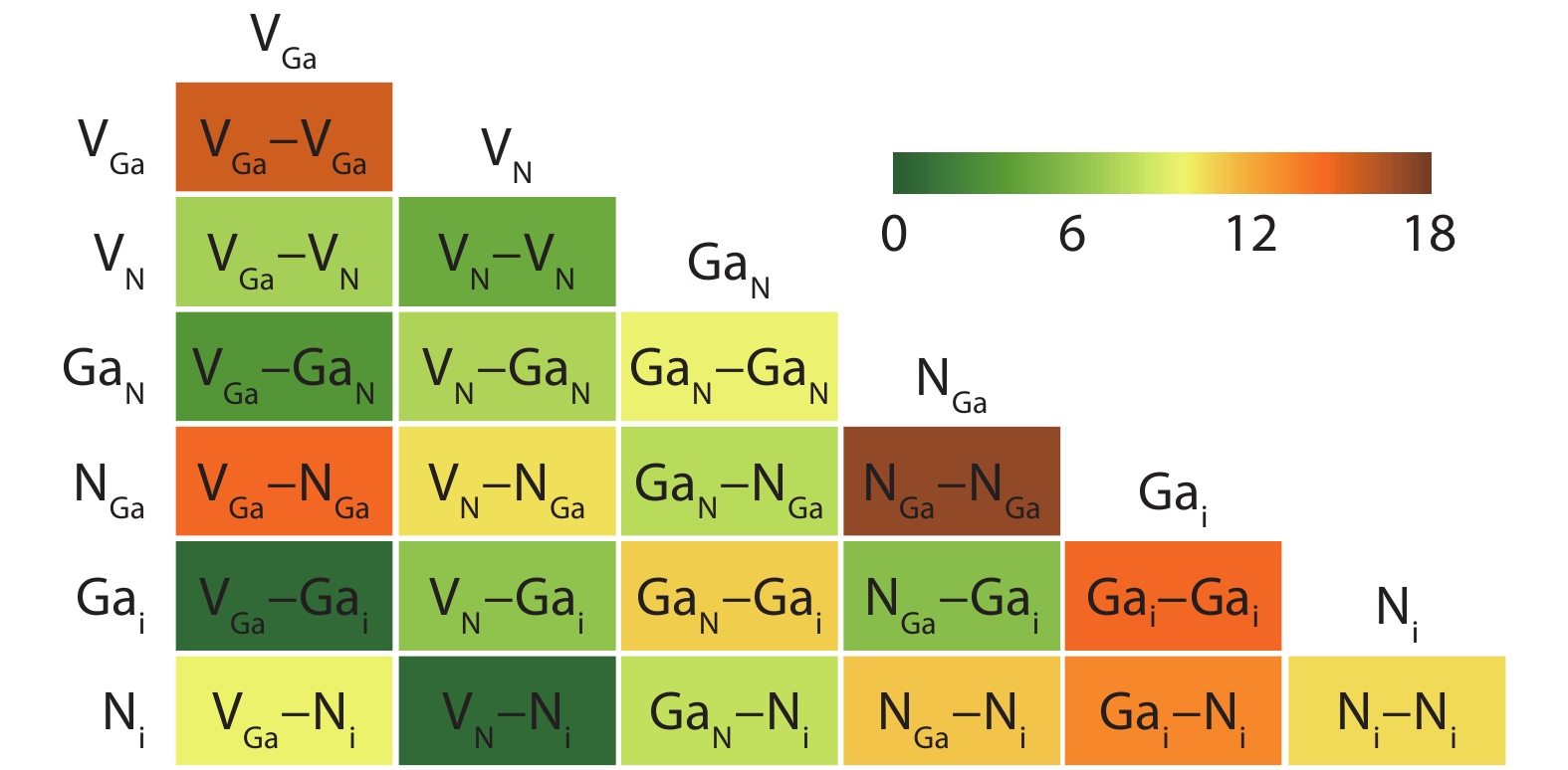
![]()
Figure 1.(Color online) The 21 defect-pairs that can be formed by two point defects in GaN. The color represents their formation energies in the neutral state (in Ga-rich GaN).
In this paper we performed a systematical study on all the 21 defect-pairs in GaN through first-principles calculations of their structures, formation energies and transition energy levels. 126 structural configurations of 21 defect-pairs are considered. Most of these defect-pairs are found to be stable with short defect-defect distances and 9 defect-pairs are identified with formation energies lower than 10 eV, so they may exist with a high concentration and play important roles in the irradiated GaN. They mainly act as donors, producing many defect levels in the band gap of GaN. Their formation energies and concentrations differ significantly in the Ga-rich and N-rich GaN, indicating that the defect formation and diffusion behavior after irradiation should be very different in the Ga-rich and N-rich GaN. Among these defect-pairs, we identified one important but overlooked defect-pair, the vacancy-pair VN–VN, which acts as a deep donor and has very low formation energies and thus high concentration in p-type and Ga-rich GaN. Its importance in limiting the p-type doping and the minority carrier lifetime is pointed out. These results about defect-pairs are fundamental for understanding the radiation damage mechanism in GaN and also directly useful for the multiscale simulation of the defect formation and diffusion processes in the irradiated GaN, e.g., using the IM3D code.
2. Calculation methods
Our first-principles calculations are performed using the density functional theory and the projector-augmented wave method[
where
3. Results and discussion
3.1. Structural configurations of defect-pairs
In the binary compound GaN, there are 6 intrinsic point defects, including two vacancies (VGa, VN), two interstitials (Gai, Ni) and two antisites (GaN, NGa). In principle, they can form 21 types of defect-pairs. As the two point defects are located on different sites, the formed defect-pairs can have many structural configurations. For each defect-pair, we construct 6 structural configurations with different defect–defect distances. Taking VN–VN as an example, its 6 different configurations are shown in Fig. 2. The distance between the two VN increases from (VN–VN)-1 to (VN–VN)-6. For (VN–VN)-1 and (VN–VN)-2, the two VN are around the same Ga and the distances are both about 3.18 Å, however, for the other four configurations, the two VN are not around the same Ga, so the distances increase to 4.51, 5.18, 5.53 Å, as listed in Table 1.
![]()
Figure 2.(Color online) Six different structural configurations of the VN–VN defect-pair (classified as Group-1). The blue balls show the locations of the two nitrogen vacancies (VN).
As a result of the equivalency of the Ga and N sites in the wurtzite structure, the structural configurations of VGa–VGa are same as those of VN–VN. Furthermore, VN–GaN, GaN–GaN, VGa–NGa and NGa–NGa also have the same structural configurations as VGa–VGa and VN–VN, because these defect-pairs are also formed on two Ga or two N sites. We classify these 6 defect-pairs as the Group-1.
In contrast, VGa–VN, VGa–GaN VN–NGa and GaN–NGa, are located on one Ga site and one N site, so they are classified as Group-2, and the distances between the two sites are listed in Table 2. The defect-pairs located on one Ga or N site and one interstitial site, including VGa–Gai, VGa–Ni, VN–Gai, VN–Ni, GaN–Gai, GaN–Ni, NGa–Gai and NGa–Ni, are classified as Group-3. The three interstitial-pairs Gai–Gai, Gai–Ni and Ni–Ni are classified as Group-4.
3.2. Defect structures relaxed using different functionals
With the structural configurations of the 21 defect-pairs, we then calculated their formation energies. The hybrid functional was shown to be more accurate in calculating the band gap of GaN and thus the formation energies and transition energy levels of defects in GaN than the GGA functional, and the calculated results agree better with the available experimental measurements[
In order to evaluate the error of our PBE + HSE method, we compared our PBE + HSE results (using GGA-PBE for structural relaxation and HSE for static calculations) to those using HSE for both the structural relaxation and static calculations for two defect-pairs VN–VN and VGa–VN. The formation energies of the two defect-pairs in 6 different configurations calculated using both the PBE-relaxed and HSE-relaxed structures are shown in Table 1. For VN–VN, the shortest-distance configuration (VN–VN)-1 is energetically the most favorable configuration with formation energies of 4.67 and 4.58 eV using the PBE- and HSE-relaxed structure, respectively. (VN–VN)-2 has an energy 0.23–0.33 eV higher, while other long-distance configurations have much higher energies, at least 1.5 eV higher. The significant energy increase from the short-distance configurations to the long-distance configurations indicates that the two VN tend to bind with each other to form a short-distance defect-pair, which is independent of the specific functionals used for the structural relaxation. For VGa–VN, (VGa–VN)-1 and (VGa–VN)-2 are energetically the most favorable and their formation energies are almost degenerate. Other long-distance configurations also have much higher energies, at least 1.6 eV higher. For both VN–VN and VGa–VN, our PBE + HSE method predicts the correct lowest-energy configurations, consistent with those predicted by the full HSE calculations. For the lowest-energy configurations, the formation energy differences between the PBE-relaxed and HSE-relaxed results are less than 0.2 eV, while for the higher-energy configurations, the formation energy differences can be as large as 0.9 eV, indicating that our calculations using the PBE-relaxed structures can predict the formation energies with an error less than 0.9 eV. Compared to the absolute value of the formation energy around 9 eV, the error is about 10%. This error is acceptable for the high-throughput exploration of defect-pairs that may form in the irradiated GaN with radiation damage.
For the lowest-energy configurations of VN–VN and VGa–VN, we further calculated the formation energies in different charge states which change with the Fermi level, as shown in Fig. 3. The comparison shows that the results for the charged defect-pairs of our PBE + HSE method are also in good agreement with those of the full HSE method (Note that the PBE- and HSE-relaxed structures differ slightly for VGa–VN, resulting in the different transition energy levels). Therefore, in the following, we will use the PBE + HSE (PBE relaxation and HSE static calculation) method to calculate the formation energies and transition energy levels of 21 intrinsic defect-pairs with different structural configurations.
![]()
Figure 3.(Color online) The formation energies of two defect-pairs VN–VN and VGa–VN in different charge states as functions of the Fermi level (in Ga-rich GaN), calculated with PBE-relaxed and HSE-relaxed structures.
3.3. Unstable defect-pairs relaxing into point defects
The calculated formation energies of 21 intrinsic defect-pairs in the neutral charge state are shown in Table 2. According to their structures, the 21 defect-pairs are classified into four groups, as mentioned in Section 3.1. For each defect-pair, 6 structural configurations with different distances between two defect sites are considered, and the distances are listed in Table 2. Both the Ga-rich and N-rich conditions are considered. For the defect-pairs with formation energies lower than 10 eV in the neutral state, we further calculated the formation energies in different charge states, as shown in Fig. 4 where the formation energies of single-site point defects are also plotted for comparison.
![]()
Figure 4.(Color online) The formation energies of (a) 6 point defects, (b) 6 defect-pairs that have the same component atoms as point defects, (c) 7 defect-pairs that cannot relax to point defects, as functions of Fermi level in Ga-rich GaN. (d–f) shows the corresponding results in N-rich GaN.
Two defect-pairs VGa–Gai and VN–Ni (Frenkel defect pair) are found to be unstable and annihilated during the structural relaxation. The structural relaxation of VGa–Gai shows that the interstitial Ga moves back to the Ga vacancy and fills the vacancy, causing the annihilation of the Frenkel defect pair, so the calculated formation energy becomes zero in Table 2 (the crystalline lattice becomes defect-free). For VGa–Gai, no matter how large the distance between the vacancy and the interstitial is, the Ga interstitial can relax back to the vacancy during the structural relaxation, so the formation energies of all the configurations are 0 in Table 2. Therefore, we can conclude that VGa–Gai cannot exist as a stable Frenkel defect pair. Four short-distance configurations (shorter than 2 Å) of VN–Ni cannot exist as stable Frenkel defect pairs either, because the interstitial N atom also relaxes back to the N vacancy site. However, when the distance between VN and Ni increases to 3.69 and 4.87 Å, the formation energies of VN–Ni increase to 7.66 and 8.42 eV, respectively, indicating that there is a barrier preventing the interstitial N from relaxing back to the vacancy site, so these VN–Ni configurations are stable Frenkel defect pairs although the distance is quite large. The origin is that the N anion is relatively small, so it can stay on the interstitial site as a metastable state when the interstitial is far from the vacancy. The case is different from that for the large Ga cation, which cannot stay on the interstitial site as a metastable state and there is no barrier preventing it from relaxing back to the vacancy site.
Different from VGa–Gai and VN–Ni which are annihilated after the structural relaxation, VGa–GaN becomes a point defect VN after the structural relaxation, because the antisite Ga moves back to the Ga vacancy. Similarly, the short-distance configuration of VN–Gai becomes a point defect GaN because the interstitial Ga moves to occupy the N vacancy during the structural relaxation. As shown in Figs. 4(a) and 4(b), VGa–GaN and VN–Gai have the same formation energies as VN and GaN, respectively. Thus, the formation energies of VGa–GaN and VN–Gai are plotted in dashed lines. Due to its large radius, the Ga atom on the N site or the interstitial site tends to relax to the vacancy site, so VGa–GaN and the short-distance VN–Gai becomes point defects and cannot exist as stable defect-pairs. When the distance between VN and Gai is larger than 3.5 Å, the Ga relaxation is prevented by a barrier, making the long-distance VN–Gai exist as a stable defect-pair.
In contrast to VGa–GaN and VN–Gai, VN–NGa and VGa–Ni can exist as stable defect-pairs. The relaxation of VN–NGa shows that the antisite N does not move to the N vacancy site. The relaxed VGa–Ni is also structurally different from VGa. Thus, the formation energies of VN–NGa and VGa–Ni differ from those of VGa and NGa, respectively, as shown in Fig. 4. The reason is that the small N atom can be accommodated by the Ga site and the interstitial site with a smaller energy cost.
For the two antisite-interstitial defect-pairs GaN–Ni and NGa–Gai, they can relax to the point defects Gai and Ni, respectively. But our structural relaxation shows that the relaxed structures of their 5 low-energy configurations are not exactly same as those of Gai and Ni, so these structures can be considered as the new structures of Gai and Ni point defects. Therefore, the formation energies of GaN–Ni and NGa–Gai in Figs. 4(b) and 4(e) are different from those of Gai and Ni in Figs. 4(a) and 4(d).
3.4. Properties of stable defect-pairs
Except the two defect-pairs that are annihilated and four defect-pairs that relax to point defects after structural relaxation, the other 15 defect-pairs are stable during the structural relaxation. As listed in Table 2, the lowest-energy configurations are generally those with short distances, and the longer-distance configurations have higher energies, indicating that the defect-pairs are stable because there is an energy barrier preventing them from separating into two isolated point defects. It should be noted that our criterion for stable defect-pairs here are different from the common criterion for stable defect-pairs. The common criterion for the thermodynamically stable defect-pairs is that the binding energy of the two point defects forming the defect-pair is negative, i.e., the formation energy of the defect-pair is lower than the sum of the formation energies of two isolated point defects. In the equilibrium state, this criterion is valid for the defect formation because the defect concentration is determined by its formation energy, and a high-energy defect-pair with a positive binding energy tends to separate into two isolated point defects, which is thermodynamically favorable. However, under the irradiation of high-energy particles, the semiconductors are in the non-equilibrium state and some high-energy defect-pairs may be formed during the collision cascade process following the primary knock-on atom (PKA) event. If these defect-pairs are not annihilated or relax to point defects after structural relaxation, and their short-distance configurations have lower energies than longer-distance configurations (producing an energy barrier), these defect-pairs can exist in the lattice for a long period and be stable dynamically, even though they are not at the thermodynamic ground state. For studying the defects in the radiation-damaged semiconductors, we adopt this criterion for the stability of defect-pairs.
Although the formation and concentration of defects are not solely determined by the formation energies in the non-equilibrium state, the formation energies are still important because they influence the defect formation and diffusion processes directly under irradiation and the values are necessary for the multiscale simulation of these processes[
![]()
Figure 5.(Color online) The transition energy levels of the 13 defect-pairs in the band gap of GaN.
In Figs. 4(b) and 4(e), the formation energies of the 6 defect-pairs that have the same component atoms as point defects are shown. As we see, the results in Fig. 4(b) are similar to those in Fig. 4(a), and Fig. 4(e) similar to Fig. 4(d). In Ga-rich GaN, the stable defect-pair VN–NGa has a formation energy around 4 eV in n-type GaN (when the Fermi level is close to CBM level) and a formation energy around 6 eV in p-type GaN (the Fermi level is close to VBM level). In N-rich GaN, the values are decreased to 3 and 5 eV respectively. Another stable defect-pair VGa–Ni has a higher formation energy, above 7 eV in Ga-rich GaN and above 4.5 eV in N-rich GaN. The two stable defect-pairs produce 7 transition energy levels in the band gap, which are quite different from the levels of the point defects VGa and NGa with the same atom composition.
In Figs. 4(c) and 4(f), the formation energies of the 7 defect-pairs that cannot relax to any point defects are shown. In Ga-rich GaN, most of the defect-pairs have formation energies in the range 4–10 eV, but one defect-pair VN–VN, has a very low formation energy, as low as 0 eV in p-type GaN. In N-rich GaN, most of the defect-pairs have formation energies in the range 4–8 eV, and VN–VN has a formation energy as low as 2.5 eV in p-type GaN. The low formation energies of these defect-pairs indicate that they may form and exist with a high concentration in the irradiated GaN because the high-energy particles and the primary knock-on atoms (PKA) can carry much higher energies and collide with other atoms to form these defect-pairs.
Among these low-energy defect-pairs, VN–VN has the lowest energy and should be the most favorable defect-pair in GaN. Its two short-distance configurations both have low formation energies, but (VN–VN)-1 with the two vacancies in two different (0001) planes is more stable than (VN–VN)-2 with the two vacancies in the same (0001) plane, and the energy difference is about 0.23 eV. In the neutral state, the formation energy of VN–VN is 4.72 eV in Ga-rich GaN and 7.16 eV in N-rich GaN. It is a donor defect, so it can be ionized to +1 and +2 charged states, then its formation energy can be decreased as the Fermi level is decreased to close to VBM in p-type GaN. In Ga-rich and p-type GaN, the +2 charged VN–VN has a formation energy around 0 eV, indicating that this defect-pair can have a very high concentration if Ga-rich GaN samples are doped into highly p-type. In N-rich GaN, the +2 charged VN–VN has a formation energy higher than 2 eV, but it’s still the lowest among all the defect-pairs. The very low formation energy and thus the easy formation of VN–VN defect-pairs have never been reported as far as we know, despite hundreds of papers about the defects in GaN have been published since 1990s[
The vacancy-pair, VGa–VN, usually known as the divacancy defect in GaN[
Another important but overlooked defect-pair for the defect diffusion in GaN is the antisite-pair GaN–NGa. We expected that this antisite-pair may be a charge-compensated defect and thus does not produce any transition energy levels in the band gap. However, our calculations showed that it is also an efficient donor, producing three donor levels in the band gap, as shown in Fig. 5. Its formation energy can be lower than 4 eV in p-type GaN, and the value is also independent of the Ga-rich or N-rich condition. Its formation energy is only higher than that of VN–VN but lower than other defect-pairs, indicating that its equilibrium concentration can be the second highest in the p-type GaN after irradiation. Our literature search shows that the properties of this antisite-pair had been seldom reported, and its importance had been overlooked. As an antisite-pair, GaN–NGa can be the intermediate state of the inter-diffusion of Ga cations and N anions after the irradiation injects high local energy in a certain region of the GaN lattice. Our calculated transition energy levels may be used to explain the photoluminescence experiments of the radiation-damaged GaN.
As shown in Figs. 4(c) and 4(f), most of the 7 defect-pairs tend to act donors. As the Fermi level is near the VBM level, they are ionized to the positive charge states and their formation energies are low, and as the Fermi level shifts up, their formation energies increase and they become unionized and even negatively charged. Therefore, a large number of donor levels are shown in Fig. 5. Only VGa–VN and NGa–Ni produce two deep acceptor levels, and can be ionized to the positive charge states with obviously lower formation energies in the n-type GaN.
Comparing the Ga-rich and N-rich conditions, we can see that two GaN-related defect-pairs, VN–GaN and GaN–GaN have formation energies lower than 8 eV in Ga-rich GaN while much higher energies above 10 eV in N-rich GaN. In contrast, two Ni-related defect-pairs, NGa–Ni and Ni–Ni, have formation energies lower than 8 eV in N-rich GaN while much higher formation energies in Ga-rich GaN. The significant differences in the formation energies and thus the concentrations of these defect-pairs indicates that the radiation-damage effects in Ga-rich and N-rich GaN samples should be very different, and a comparison study of Ga-rich and N-rich GaN samples is necessary for studying the effects of various radiations on GaN devices.
4. Conclusions
The 21 defect-pairs formed by two point defects in GaN are studied using the first-principles calculations. For each defect-pair, 6 structural configurations with different defect-defect distances are considered, and 126 structural configurations of 21 defect-pairs are studied in total. The calculations showed: (i) after structural relaxation, 2 defect-pairs VGa–Gai and VN–Ni (Frenkel defect pair) are annihilated and 4 defect-pairs VGa–GaN and VN–Gai, GaN–Ni and NGa–Gai become point defects, while the other 15 defect-pairs remain as defect-pairs with short defect-defect distances; (ii) most of these defect-pairs have lower formation energies when the defect-defect distances are small, indicating that there is an energy barrier preventing the separation of the defect-pairs into two isolated point defects and the defect-pairs can be stable once formed during the irradiation of high-energy particles; (iii) 9 stable defect-pairs have their formation energies lower than 10 eV in the neutral charge state, so they form and play important role in influencing the properties of radiation-damaged GaN; (iv) the vacancy-pair VN–VN is found to have very low formation energies and thus high concentration, especially in p-type and Ga-rich GaN. It can be an important limiting defect to the p-type doping and also causes serious non-radiative recombination because it produces deep donor levels. The high concentration and importance of VN–VN in p-type and Ga-rich GaN has been overlooked in the past three decades; (v) most of these defect-pairs act as donors, and their formation energies fall in the range 4-8 eV and differ significantly in the Ga-rich and N-rich GaN, indicating that the defect formation and diffusion behavior in the Ga-rich and N-rich GaN after irradiation should be quite different and a comparison study is necessary. Our calculated properties of these defect-pairs provide fundamental data for the simulation of defect formation and diffusion in the irradiated GaN. Further study on the important defect-pairs that we identified, including VN–VN in Ga-rich and p-type GaN and GaN–NGa in the radiation-damaged GaN, are called for.
Acknowledgements
The authors thank Profs. Yongsheng Zhang and Yonggang Li for telling us the importance of defect-pairs in the simulation of radiation damage. This work was supported by the Science Challenge Project (TZ2018004), National Natural Science Foundation of China (NSFC) under grant Nos. 61722402 and 91833302, National Key Research and Development Program of China (2016YFB0700700), Shanghai Academic/Technology Research Leader (19XD1421300), Fok Ying Tung Education Foundation (161060) and the Fundamental Research Funds for the Central Universities.
References
[1] S Nakamura, T Mukai, M Senoh. Candela-class high-brightness InGaN/AlGaN double-heterostructure blue-light-emitting diodes. Appl Phys Lett, 64, 1687(1994).
[2] M H Kim, M F Schubert, Q Dai et al. Origin of efficiency droop in GaN-based light-emitting diodes. Appl Phys Lett, 91, 183507(2007).
[3] S Pimputkar, J S Speck, S P DenBaars et al. Prospects for LED lighting. Nat Photonics, 3, 180(2009).
[4] S T Sheppard, K Doverspike, W L Pribble et al. High-power microwave GaN/AlGaN HEMTs on semi-insulating silicon carbide substrates. IEEE Electron Device Lett, 20, 161(1999).
[5] S J Pearton, R Deist, F Ren et al. Review of radiation damage in GaN-based materials and devices. J Vac Sci Technol A, 31, 050801(2013).
[6] J Wang, P Mulligan, L Brillson et al. Review of using gallium nitride for ionizing radiation detection. Appl Phys Rev, 2, 031102(2015).
[7] S J Pearton, F Ren, E Patrick et al. Review-ionizing radiation damage effects on GaN devices. ECS J Solid State Sci Technol, 5, Q35(2015).
[8] S J Pearton, Y S Hwang, F Ren. Radiation effects in GaN-based high electron mobility transistors. J Mater, 67, 1601(2015).
[9] S M Khanna, D Estan, A Houdayer et al. Proton radiation damage at low temperature in GaAs and GaN light-emitting diodes. IEEE Trans Nucl Sci, 51, 3585(2004).
[10] K Lorenz, M Peres, N Franco et al. Radiation damage formation and annealing in GaN and ZnO. Proc SPIE(2011).
[11] A Y Polyakov, N B Smirnov, A V Govorkov et al. Neutron radiation effects in epitaxially laterally overgrown GaN films. J Electron Mater, 36, 1320(2007).
[12]
[13] J Nord, K Nordlund, J Keinonen. Molecular dynamics study of damage accumulation in GaN during ion beam irradiation. Phys Rev B, 68, 184104(2003).
[14] F J Bryant, E Webster. Threshold energy for atomic displacement in cadmium telluride. Phys Status Solidi B, 21, 315(1967).
[15] F J Bryant, A F J Cox, F C Frank. Experimental and calculated atomic displacement threshold energies for binary semiconductors. Proceedings of the Royal Society of London, Ser A, 310, 319(1969).
[16] H J Von Bardeleben, J L Cantin, U Gerstmann et al. Identification of the nitrogen split interstitial (N-N)N in GaN. Phys Rev Lett, 109, 206402(2012).
[17] C G Van de Walle, J Neugebauer. First-principles calculations for defects and impurities: Applications to III-nitrides. J Appl Phys, 95, 3851(2004).
[18] M A Reshchikov, H Morkoç. Luminescence properties of defects in GaN. J Appl Phys, 97, 061301(2005).
[19] J L Lyons, A Alkauskas, A Janotti et al. First-principles theory of acceptors in nitride semiconductors. Phys Status Solidi B, 252, 900(2015).
[20] J L Lyons, C G Van de Walle. Computationally predicted energies and properties of defects in GaN. npj Comp Mater, 3, 12(2017).
[21] A Y Polyakov, I H Lee. Deep traps in GaN-based structures as affecting the performance of GaN devices. Mater Sci Eng R, 94, 1(2015).
[22] T Mattila, R M Nieminen. Point-defect complexes and broadband luminescence in GaN and AlN. Phys Rev B, 55, 9571(1997).
[23] I C Diallo, D O Demchenko. Native Point defects in GaN: a hybrid-functional study. Phys Rev Appl, 6, 064002(2016).
[24] Y G Li, Y Yang, M P Short et al. IM3D: A parallel Monte Carlo code for efficient simulations of primary radiation displacements and damage in 3D geometry. Sci Rep, 5, 18130(2015).
[25] L J Sham. Self-consistent equations including exchange and correlation effects. Phys Rev, 140, A1138(1965).
[26] G Kresse, D Joubert. From ultrasoft pseudopotentials to the projector augmented-wave method. Phys Rev B, 59, 1758(1999).
[27] P E Blöchl. Projector augmented-wave method. Phys Rev B, 50, 17953(1994).
[28] G Kresse, J Furthmüller. Efficient iterative schemes for ab initio total-energy calculations using a plane-wave basis set. Phys Rev B, 54, 11169(1996).
[29] J P Perdew, K Burke, M Ernzerhof. Generalized gradient approximation made simple. Phys Rev Lett, 77, 3865(1996).
[30] J Heyd, G E Scuseria, M Ernzerhof. Erratum: “Hybrid functionals based on a screened Coulomb potential” [J. Chem. Phys. 118, 8207(2003)]. J Chem Phys, 124, 219906(2006).
[31] J Heyd, G E Scuseria, M Ernzerhof. Hybrid functionals based on a screened Coulomb potential. J Chem Phys, 118, 8207(2003).
[32] B Monemar. Fundamental energy gap of GaN from photoluminescence excitation spectra. Phys Rev B, 10, 676(1974).
[33] S Lany, A Zunger. Assessment of correction methods for the band-gap problem and for finite-size effects in supercell defect calculations: Case studies for ZnO and GaAs. Phys Rev B, 78, 235104(2008).
[34] G Makov, M C Payne. Periodic boundary conditions in ab initio calculations. Phys Rev B, 51, 4014(1995).
[35] J L Lyons, A Janotti, C G Walle. Carbon impurities and the yellow luminescence in GaN. Appl Phys Lett, 97, 152108(2010).
[36] C Freysoldt, B Grabowski, T Hickel et al. First-principles calculations for point defects in solids. Rev Mod Phys, 86, 253(2014).

Set citation alerts for the article
Please enter your email address
© Copyright 2018-2021 | Chinese Laser Press. All Rights Reserved 沪ICP备15018463号-20