• Matter and Radiation at Extremes
  • Vol. 4, Issue 4, 045403 (2019)
Yudan He1, Lei Jin1, Jiqiang Zhang1, Bingchi Luo1, Kai Li1, Weidong Wu1、2、3, and Jiangshan Luo1、2、a)
Author Affiliations
  • 1Research Center of Laser Fusion, Chinese Academy of Engineering Physics, Mianyang 621900, China
  • 2Science and Technology on Plasma Physics Laboratory, Mianyang 621900, China
  • 3IFSA Collaborative Innovation Center, Shanghai Jiao Tong University, Shanghai 200240, China
  • show less
    DOI: 10.1063/1.5087112 Cite this Article
    Yudan He, Lei Jin, Jiqiang Zhang, Bingchi Luo, Kai Li, Weidong Wu, Jiangshan Luo. Thickness dependence of microstructure and properties in Be2C coatings as a promising ablation material[J]. Matter and Radiation at Extremes, 2019, 4(4): 045403 Copy Citation Text show less
    XPS spectra of Be2C coating: (a) wide scan; (b) Be1s core levels; (c) C1s core levels.
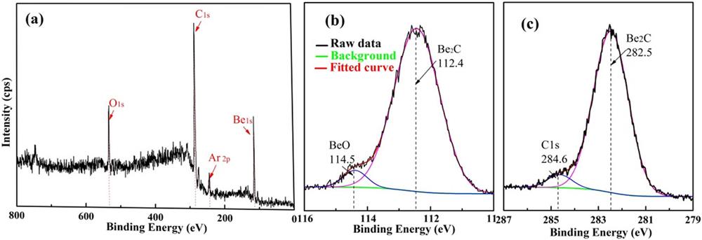
    Fig. 1. XPS spectra of Be2C coating: (a) wide scan; (b) Be1s core levels; (c) C1s core levels.
    XRD patterns of Be2C coatings of various thicknesses.
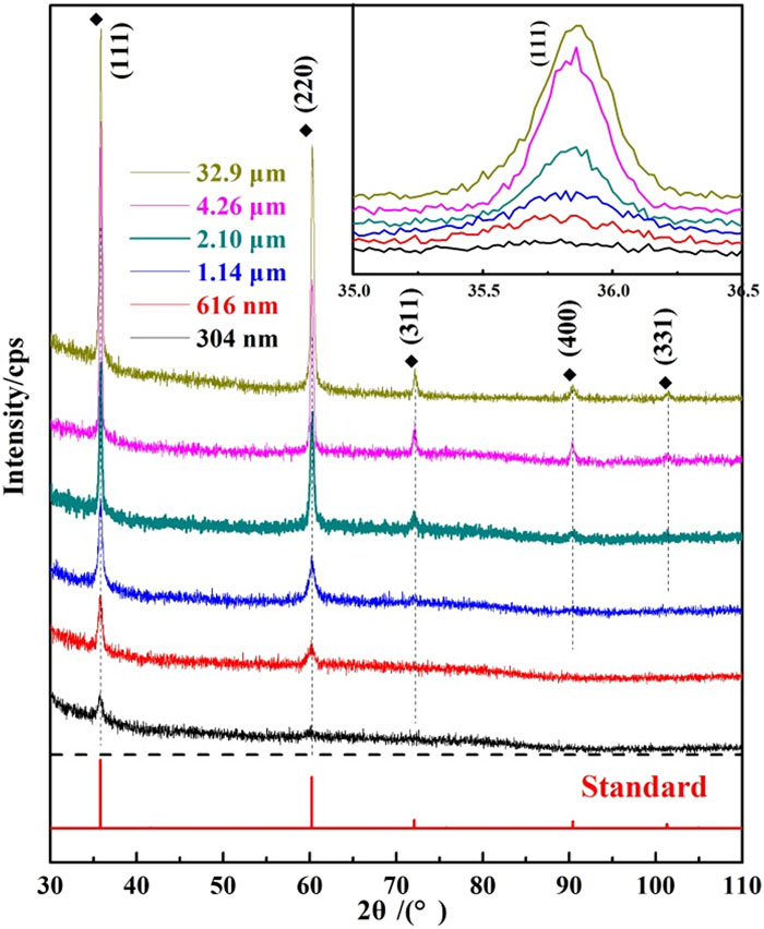
    Fig. 2. XRD patterns of Be2C coatings of various thicknesses.
    Fractured cross-sectional morphologies of Be2C films of various thicknesses.
    Fig. 3. Fractured cross-sectional morphologies of Be2C films of various thicknesses.
    Partial surface topography of Be2C films obtained from an optical profiler: (a) 304 nm; (b) 1.14 µm; (c) 4.26 µm. Typical defect morphologies: (d) top view; (e) magnified view; (f) cross-sectional view.
    Fig. 4. Partial surface topography of Be2C films obtained from an optical profiler: (a) 304 nm; (b) 1.14 µm; (c) 4.26 µm. Typical defect morphologies: (d) top view; (e) magnified view; (f) cross-sectional view.
    Optical transmittance spectra of Be2C films of different thicknesses. The inset shows a typical optical image of a film sample.
    Fig. 5. Optical transmittance spectra of Be2C films of different thicknesses. The inset shows a typical optical image of a film sample.
    Plots of (αhν)1/2 vs hν and extrapolation to determine the optical bandgap Eg for Be2C films of different thicknesses.
    Fig. 6. Plots of (αhν)1/2 vs and extrapolation to determine the optical bandgap Eg for Be2C films of different thicknesses.
    Base pressure<1.0 × 10⁻⁵ Pa
    Operating pressure5 mTorr
    Heating temperature600 °C
    CH4 (%)6
    Sputtering power2 × 180 W
    Deposition time1–120 h
    Table 1. Experimental parameters for deposition of Be2C films.
    Deposition time (h)Thickness (nm)TC(111)D (nm)Ra (nm)r (nm/h)ρ (g/cm3)
    13040.6315.41.453042.19
    26160.6217.31.603082.23
    41 1400.6017.01.182852.27
    82 1000.4926.43.532632.24
    164 2600.5831.64.802662.31
    12032 9000.5128.38.632742.29
    Table 2. Deposition time, coating thickness, texture coefficient TC(111), average crystallite size D, surface roughness Ra, deposition rate r, and density ρ of Be2C films of different thicknesses.
    Yudan He, Lei Jin, Jiqiang Zhang, Bingchi Luo, Kai Li, Weidong Wu, Jiangshan Luo. Thickness dependence of microstructure and properties in Be2C coatings as a promising ablation material[J]. Matter and Radiation at Extremes, 2019, 4(4): 045403
    Download Citation