Abstract
Beryllium carbide (Be2C) thin films have proven to be promising ablation materials, but the properties of Be2C coatings of the greater thickness required for inertial confinement fusion capsules are still unknown. In this work, Be2C coatings of various thicknesses (0.3–32.9 μm) are prepared by DC reactive magnetron sputtering. The influence of thickness on crystal properties, microstructure, and optical properties is investigated. The results indicate that the crystallinity of polycrystalline Be2C films improves with increasing thickness, while the grain size (~5 nm) and texture properties (without a preferred orientation) have only a weak dependence on thickness. A uniform featureless microstructure and smooth surface (root mean square roughness ~8 nm) are observed even in thick (32.9 μm) films, despite the presence of defects induced by contaminants. High densities (2.19–2.31 g/cm3) and high deposition rates (~270 nm/h) are realized, with the latter corresponding to the upper limit for the fabrication of Be2C coatings by magnetron sputtering. The transmittance of the films in the near-infrared region remains at a high level (>80%) and has only a weak dependence on thickness, while the transmittance in the visible region decreases with increasing thickness. In addition, the optical bandgap is estimated to be about 1.9 eV and decreases with increasing thickness owing to the presence of defects.I. INTRODUCTION
The realization of ignition is of great importance for inertial confinement fusion (ICF). A variety of physical processes (implosion velocity, instability, compression ratio, and compression symmetry, among others) will affect the implosion.1–3 This imposes a number of requirements on the properties of the ablative materials, such as low atomic number, smooth surface, uniform structure, and high density.3 Beryllium, hydrocarbon (CH), and high-density carbon (HDC) are the three preferred ablators owing to their respective superior properties.4–7 Beryllium has the highest ablation velocity.8 HDC provides a high compression ratio, resulting from its high density (3.5 g/cm3).9,10 CH allows easy characterization (because of its transparency in the visible–infrared region), and techniques for its fabrication are more mature.8 Experiments with Be, HDC, and CH capsules have been performed on the National Ignition Facility (NIF).7,9–11 Unfortunately, fusion ignition has not yet been achieved. Therefore, further research on potential ablative materials is of particular importance.
One such material is beryllium carbide (Be2C),12–15 which possesses a high density (2.44 g/cm3, which is higher than those of Be and CH) and a low atomic number (4.67, which is lower than that of HDC). As a yellow–brown transparent crystal, it should be possible to characterize Be2C capsules using the same techniques as for CH capsules. In conclusion, Be2C combines the advantages of Be, HDC, and CH, and may also have a more balanced ablation performance.13 However, owing to a lack of high-quality Be2C targets, its performance under ablation has not been evaluated experimentally.
Be2C coatings were first prepared in the 1990s by plasma polymerization and RF reactive sputtering.14,15 However, some fatal drawbacks limited their further development, as described previously.12,13 Recently, thanks to improvements in coating technology, a practical method (improved DC reactive magnetron sputtering) for fabricating Be2C coatings has been reported.13 Experimental parameters such as flow ratios and growth temperatures have been studied to analyze their influence. High-purity Be2C coatings were obtained and were found to exhibit superior properties (including a smooth surface, a uniform structure, and a high density). However, these studies focused mainly on films of thickness less than 2 µm, which are much thinner than those required for ICF capsules (∼160 µm for Be7,16). It is not known at present whether the excellent properties of Be2C thin films can be retained at large thicknesses. The microstructures and properties of coatings generally depend on their thickness.7,17,18 For example, with increasing thickness the microstructure of a Be coating changes from a columnar crystalline into a twisted form,7 as a result of which it becomes more irregular and the surface roughness increases. Therefore, a systematic investigation of the effect of thickness is of great importance for evaluating Be2C as an ablation material, although to date there have been no reports in the literature of such studies.
In the present work, Be2C films of different thicknesses are deposited, and the effects of thickness on crystallinity, microstructure, surface morphology, and other properties are analyzed. The results show that the excellent performances of Be2C can be retained as the thickness increases to large values. We believe that this study represents a significant step forward in the study of Be2C and will aid significantly in advancing the application of Be2C films in ICF.
II. EXPERIMENTAL
Be2C films of different thicknesses were deposited on K9 substrates in an Ar/CH4 plasma using a homemade DC reactive magnetron sputtering system. Two round magnetrons with a Be target (purity > 98.5%, 76 mm in diameter) were symmetrically positioned above the sample holder. The distance between the substrate and targets was ∼90 mm. Ar was introduced behind the sputtering target, while CH4 was introduced near the substrate to reduce the risk of target poisoning. Experimental parameters were determined by repeated optimization to ensure a pure composition of Be2C and are listed in Table I. The deposition time was varied over a large range from 1 h to 120 h to obtain films of different thicknesses: 304 nm, 616 nm, 1140 nm, 2100 nm, 4260 nm, and 32 900 nm. Before deposition, targets were presputtered with Ar+ to remove contaminants and expose fresh Be surfaces. The heating temperature was decreased as slowly as possible (1 °C/min) to prevent the films from fracturing after deposition. The substrates were rotated at 6 rev/min throughout the process to improve the uniformity of the films.
| Base pressure | <1.0 × 10⁻⁵ Pa |
| Operating pressure | 5 mTorr |
| Heating temperature | 600 °C |
| CH4 (%) | 6 |
| Sputtering power | 2 × 180 W |
| Deposition time | 1–120 h |
Table 1. Experimental parameters for deposition of Be2C films.
The chemical composition was determined by X-ray photoelectron spectroscopy (XPS), the phase composition and crystalline properties by glancing-incidence X-ray diffraction (GIXRD), the microstructure by SEM, the surface roughness by an optical profiler, the density by a precision balance, and the optical transmittance by a double-beam spectrophotometer.
III. RESULTS AND DISCUSSION
A. Chemical composition
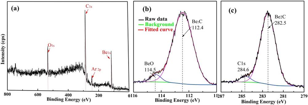
The chemical composition of a Be2C film of thickness 1140 nm was determined by XPS using an Mg–Kα (1253.6 eV) source. To eliminate the effect of surface contaminants, the film was etched by Ar+ until the survey spectrum remained stable. The survey spectra and the high-resolution spectra of Be1s and C1s core levels are shown in Fig. 1. Only peaks corresponding to Be, C, O, and Ar are observed [Fig. 1(a)], which confirms the chemical purity of the film. The O stems from oxidation during deposition, and the Ar is a residue from the Ar+ etching and the sputtering process. High-resolution spectra were used to identify the chemical states and to calculate their corresponding contents. Deconvolution of the Be1s peak19 [Fig. 1(b)] shows a dominant peak at 112.5 eV (assigned to Be2C, ∼95%) and a much weaker peak at 114.6 eV (attributed to BeO). Similarly, the C1s peak19 [Fig. 1(c)] consists of a dominant peak at 282.4 eV (Be2C, ∼95%) and a slight peak at 284.6 eV (C–C). The atomic ratio of Be to C evaluated from peak areas and atomic sensitivity factors20 is 2.11, close to the stoichiometry (2) of Be2C. These results indicate that the 1140 nm film is mainly composed of Be2C. Since the experimental conditions were not altered for the production of films of different thicknesses, it can be assumed that they have similar compositions.

Figure 1.XPS spectra of Be2C coating: (a) wide scan; (b) Be1s core levels; (c) C1s core levels.
B. Phase composition
GIXRD (Cu–Kα 1.540 56 Å) was performed to study the phase and crystalline properties of the films. The scanning step was 0.02° and the scanning speed 0.5 s/step. The GIXRD patterns of the samples together with standard Be2C powder XRD spectra (PDF-33-0191) are presented in Fig. 2. The main characteristic peaks (111) and (220) of Be2C appear at approximately 35.8° and 60.2° in all samples, while no signals from any secondary phases are detected. This indicates that Be2C is the predominant phase in films of different thicknesses, which is consistent with the XPS analysis. Moreover, the diffraction peaks become sharper and their intensity is enhanced as the thickness increases from 0.3 µm to 32.9 µm, indicating a significant improvement in crystallinity.
Figure 2.XRD patterns of Be2C coatings of various thicknesses.
The texture coefficient (TC) is introduced to evaluate the textural properties of the films and is calculated as follows:21where is the intensity of the (hkl) plane in the experimental XRD patterns and is the intensity in the standard powder XRD spectra. In this work, the strongest peak (111) and substrong peak (220) are adopted to calculate the TC. For randomly oriented samples (such as powders), TC(111) = 0.5. The TC(111) values of Be2C films of different thicknesses are listed in Table II. It can be seen that the thickness does not have a strong effect on TC(111), which ranges from 0.49 to 0.63 (close to 0.5) as the thickness varies. This suggests that Be2C films of different thicknesses do not exhibit a preferred orientation (i.e., they are isotropic). In contrast, Be films always exhibit strong anisotropy.22 This leads to asymmetric ablation, which is harmful to ablative materials. In addition, the consistency of the XRD patterns of films of different thicknesses also reflects the uniformity of Be2C films in the vertical direction.
| Deposition time (h) | Thickness (nm) | TC(111) | D (nm) | Ra (nm) | r (nm/h) | ρ (g/cm3) |
|---|
| 1 | 304 | 0.63 | 15.4 | 1.45 | 304 | 2.19 |
| 2 | 616 | 0.62 | 17.3 | 1.60 | 308 | 2.23 |
| 4 | 1 140 | 0.60 | 17.0 | 1.18 | 285 | 2.27 |
| 8 | 2 100 | 0.49 | 26.4 | 3.53 | 263 | 2.24 |
| 16 | 4 260 | 0.58 | 31.6 | 4.80 | 266 | 2.31 |
| 120 | 32 900 | 0.51 | 28.3 | 8.63 | 274 | 2.29 |
Table 2. Deposition time, coating thickness, texture coefficient TC(111), average crystallite size D, surface roughness Ra, deposition rate r, and density ρ of Be2C films of different thicknesses.
The average grain size is calculated by Scherrer’s formula , where θ is the Bragg angle, λ is the X-ray wavelength, and β is the full width at half maximum (FWHM) of the (111) peak. The variation of the grain size among films of different thicknesses can be seen from Table II. It gradually increases from 15.4 nm to 31.6 nm as the thickness increases from 304 nm to 4.26 µm. It then remains stable despite an increase in thickness to 32.9 µm. The grain size of Be2C coatings is smaller than those of HDC coatings (70 nm)23 and Be coatings (>100 nm)22 and is within the requirements for ICF capsules.24 Fine grains improve uniformity, which reduces asymmetry and Rayleigh–Taylor instability during ablation. Therefore, the weak dependence of grain size on film thickness is considered to be one of the essential advantages of Be2C as an ablation material, especially given that ICF capsules are often thicker than 100 µm. By contrast, the grain size of Be coatings grows rapidly with increasing thickness, reaching the scale of the thickness in the vertical direction.22,25 Indeed, grain refinement is one of the key issues encountered when Be is used as an ablation material.
C. Microstructure and morphology
Figure 3 shows the cross-sectional morphologies of the various Be2C films, with the measured thicknesses indicated on the SEM images. It can be seen that the films have a compact uniform microstructure and a clear interface with the substrate. However, some subtle microstructural evolution is revealed on careful examination. The film with a thickness of 304 nm presents a small rod grain (diameter ∼30 nm) structure [Fig. 3(a)]. With increasing thickness, the rod grains gradually merge. Interestingly, instead of leading to the development of coarse columnar grains (as in Be coatings), this results in a denser and uniform morphology [Figs. 3(b) and 3(c)]. The films become more uniform and exhibit a featureless structure [Figs. 3(d) and 3(e)] as the thickness increases to 2.1–4.26 µm. The films maintain this uniform structure even when the thickness reaches 32.9 µm [Fig. 3(f)]. By contrast, Be coatings exhibit a coarse columnar grain structure, and the columnar grains grow bigger and bigger with increasing film thickness.22 This might indicate that Be2C films tend to form a uniform structure even at greater thicknesses. Such a uniform structure is desirable for ablative materials because it has a beneficial effect on the isotropy of ablation and decreases perturbations during spherical compression.
Figure 3.Fractured cross-sectional morphologies of Be2C films of various thicknesses.
Based on the thickness measured by SEM, the deposition rates are calculated and are shown as a function of deposition time in Table II. The deposition rate is ∼300 nm/h in the first 2 h. It then gradually decreases to ∼270 nm/h and remains close to this value at later times. This deposition rate is more than four times higher than the maximum deposition rate (∼56 nm/h) obtained with RF reactive magnetron sputtering reported in the literature.14 It can be improved further by increasing the number of sputtering magnetrons. A higher deposition rate is beneficial for the deposition of ICF capsules.
A high density is a desirable characteristic of ablative materials, since it provides a higher X-ray absorption efficiency.7,8 The density of a Be2C coating can be calculated as , where m is the mass of the coating (measured by a precision balance with a precision of 1 µg), s is its area, and d is its thickness. The calculated densities are shown in Table I. Thin films (<1 µm) have lower densities. With increasing thickness, the films become denser and reach a maximum density of 2.31 g/cm3 (approximately 95% of the theoretical density, 2.44 g/cm3).
The variations of deposition rates and densities with thickness might be related to the microstructural evolution from a rod grain structure to a dense uniform structure. During deposition, the coatings are subjected to two thermal effects, one from the heating source and the other due to sputtering. The contribution from the heating source remains constant at a fixed heating temperature, provided that sufficient time has been allowed for a steady state to be reached before deposition commences. By contrast, the sputtering thermal effect (originating from intense particle bombardment by, for example, Ar+ ions, electrons, and Be and C atoms) initially becomes stronger with increasing deposition time, although, for longer durations of deposition, a steady state is reached. Thus, the sputtered atoms acquire more energy, which increases the rate of atomic migration, thereby favoring crystalline growth and promoting the formation of a dense uniform structure.
The normal surfaces of the films are so smooth that no characteristic morphology can be observed by SEM. Figures 4(a)–4(c) show the partial surface topography of Be2C films measured by an optical profiler (White Light Interferometry). On the whole, the films exhibit a smooth platform, with only a few nanometer-size fluctuations. The surface roughness is evaluated over a 0.9 × 1.2 mm2 area and is given in Table II. The root mean square (rms) roughness decreases from 1.45 nm to 1.18 nm as the thickness increases from 304 nm to 1140 nm. This could be associated with the transformation from a rod grain structure to a dense uniform structure, since a rod grain structure results in a rougher surface. However, with further increases in film thickness, the rms roughness gradually increases. It is 4.80 nm for a thickness of 4.26 µm and is 8.63 nm when the thickness reaches 32.9 µm. This increased roughness could be attributed to the presence of nodular defects.
Figure 4.Partial surface topography of Be2C films obtained from an optical profiler: (a) 304 nm; (b) 1.14 µm; (c) 4.26 µm. Typical defect morphologies: (d) top view; (e) magnified view; (f) cross-sectional view.
Figure 4(d) shows the top-view morphology, which includes several nodular defects. Figure 4(e) is the magnified view of one of these defects. As can be seen, they exhibit a stacked circular morphology with diameters ranging from hundreds of nanometers to several micrometers. Despite the presence of defects, the platform is smooth and with no characteristic morphology on SEM, as already mentioned. The cross-sectional morphology of the nodular defects can be obtained by cleaving them under a microscope. As shown in Fig. 4(f), these defects possess a radiating cone-shaped structure. This structure originates from a small point (at the bottom or interior surface of the coating), and its top sticks out from the upper or outer surface. From the cross-sectional view, we can infer that the defects are caused by the presence of small particles, which may have been introduced by contamination from the substrate and by the deposition process (an unstable arc discharge). During deposition, small particles act as nuclei, which are thermodynamically favorable sites at which the incoming atoms can accumulate. This results in preferential growth of small particles into radiating cone-shaped nodular defects. The positions of the original particles determine the size of the defects. For thicker films, the longer duration of deposition results in a higher probability of contamination by small particles, which further induces a rougher surface.
A smooth surface and uniform structure are always desirable properties for an ablative material. Defects are detrimental to ablation because they not only act as seeds for Rayleigh–Taylor instability, but also destroy the isotropy of the ablation process. An analysis of their origin suggests that defects can be reduced by improving the cleanliness of the substrate sand the stability of the sputtering process. Despite the presence of defects, however, the roughness of Be2C coatings is still lower than that of Be coatings25 and within the requirements for ICF capsules.24 The low surface roughness of Be2C films indicates that Be2C is more likely to form a smooth surface than Be.
D. Optical properties
Optical transparency in the visible–infrared region is one of the advantages of Be2C as an ablative material. The inset in Fig. 5 shows a typical optical image of a Be2C coating (2.10 µm), which is yellow–brown in color. The transmittance and reflectance spectra of Be2C films with different thicknesses were recorded by a double-beam spectrophotometer. Figure 5 shows optical transmittance spectra. Oscillating fringes occur in both transmittance and reflectance spectra as a result of interference between light reflected from the film surface and that reflected from the interface with the substrate. The interference fringes become stronger with increasing thickness as the thickness becomes comparable to the wavelength.
Figure 5.Optical transmittance spectra of Be2C films of different thicknesses. The inset shows a typical optical image of a film sample.
In the UV–visible region, the absorption edge is redshifted and the average transmittance decreases with increasing thickness. This result can be attributed to two factors. One is the Beer–Lambert law26 (stronger absorption arising from longer optical paths in thicker coatings). The other is enhanced scattering by defects. In the infrared region (especially >1000 nm), the transmittance [using the envelope method to exclude the influence of the interference fringes (not shown)] has only a weak dependence on the film thickness and remains at a high level (>80%). The transmittance in the visible and infrared region indicates that it should be feasible not only to characterize D-T fuel contained in Be2C capsules by optical methods, but also to homogenize this fuel using infrared heating.
The absorption coefficient α is obtained from the transmittance (T) and reflectance (R) spectra and the film thickness d as follows:The optical bandgap Eg is estimated using the Tauc model:27, where A is the band edge constant, hν is the photon energy, and n characterizes the nature of the band transition (n = 1/2 for an indirect allowed transition like that for Be2C).13 The relationship between (αhν)1/2 and hν is shown in Fig. 6. By extrapolating the linear portion to (αhν)1/2 = 0, the optical bandgaps of Be2C films are obtained and are also shown in Fig. 6. For films with thickness greater than 1.14 µm, the optical bandgap decreases slightly (from 1.99 eV to 1.95 eV) with increasing thickness, which is in agreement with other work.28 These values are larger than the theoretical bandgap (1.2 eV) of Be2C,29 but close to the experimental data (∼2 eV) from electron energy loss spectra30 as well as the values found in previous work.13 As the thickness increases further, there is a rapid decrease in the bandgap, which becomes 1.40 eV at a thickness of 4.26 µm. Previous studies31,32 revealed that many factors (e.g., chemical composition, crystallinity, defects, the quantum size effect, and the Moss–Burstein effect) can lead to anomalous variations in the bandgap. In the present work, all films were deposited under a constant sputtering condition, so they had the same chemical composition. The thickness of the Be2C films (even the thinnest) is much greater than the exciton Bohr radius,31 and so quantum confinement effects cannot occur. The carrier concentration has been measured to evaluate the Moss–Burstein effect. The films exhibit n-type conductivity with carrier density in the range (1–5) × 1016 cm−3, which is far below the density required to cause the Moss–Burstein effect (∼1019 cm−3).31 Thus, the Moss–Burstein effect can be excluded, and therefore the variation of the bandgap can be attributed to the crystallinity and/or to defects. For thinner films (≤1.14 µm), the improvement in crystallinity (as verified by XRD) should play a dominant role in decreasing the bandgap. When the thickness exceeds 1.14 µm, the crystallinity remains stable, but the bandgap decreases dramatically. This decrease must have a different origin. We note that with the thickness exceeding 1.14 µm, the number of defects obviously will increase, and thus the decrease in the bandgap can be attributed to the presence of defects.
Figure 6.Plots of (αhν)1/2 vs hν and extrapolation to determine the optical bandgap Eg for Be2C films of different thicknesses.
IV. CONCLUSIONS
Be2C films with various thicknesses (0.3–32.9 µm) were deposited on K9 substrates by DC reactive magnetron sputtering, which allowed a detailed investigation of the effects of film thickness on structural evolution and optical properties. XPS revealed the compositional purity of the Be2C films. All the films, regardless of thickness, consisted of polycrystalline Be2C without a preferred orientation. However, the crystallinity did significantly improve with increasing thickness. The grain size remained almost stable, and was about 25 nm when the thickness exceeded 4.26 µm, although a slight increase occurred with increasing thickness for the thinner films. The thinner films exhibited a small rod grain structure and a smooth surface (Ra < 5 nm). As the thickness increased, the structure became uniform and featureless, but the surface roughness increased owing to defects induced by contaminants. The density of the films was 2.19–2.31 g/cm3. The deposition rate reached ∼270 nm/h, which is the upper limit for the fabrication of Be2C coatings by magnetron sputtering. The transmittance of the films in the visible region decreased with increasing thickness, whereas that in the near-infrared region had only a weak dependence on the thickness and remained at a high level (>80%). In addition, the optical bandgap was estimated to be about 1.9 eV and decreased with increasing thickness owing to the presence of defects.
These results indicate that Be2C is inclined to form polycrystalline coatings with no preferred orientation and with fine grains, uniform microstructure, smooth surface, high density, and optical transparency, and that these properties have only a weak dependence on film thickness. All of these properties are beneficial to the ablation performance of ICF capsules made using such films, and so the results obtained here are encouraging with regard to the application of Be2C in ICF.
References
[1] Z. C. Li, K. Lan, X. F. Xie, W. Y. Huo, J. Liu et al. Progress in octahedral spherical hohlraum study. Matter Radiat. Extremes, 1, 8-27(2016).
[2] B. A. Hammel1. The NIF ignition program: Progress and planning. Plasma Phys. Controlled Fusion, 48, B497-B506(2006).
[3] B. A. Hammel, D. S. Clark, D. A. Callahan, J. D. Lindl, S. W. Haan, J. D. Salmonson et al. Point design targets, specifications, and requirements for the 2010 ignition campaign on the National Ignition Facility. Phys. Plasmas, 18, 051001(2011).
[4] D. Clark, A. B. Zylstra, S. A. Yi, A. L. Kritcher, S. Haan et al. Comparison of plastic, high density carbon, and beryllium as indirect drive NIF ablators. Phys. Plasmas, 25, 056309(2018).
[5] S. W. Haan, A. L. Kritcher, S. A. Yi, A. B. Zylstra, D. S. Clark et al. Capsule physics comparison of National Ignition Facility implosion designs using plastic, high density carbon, and beryllium ablators. Phys. Plasmas, 25, 032703(2018).
[6] S. A. Yi, D. C. Wilson, J. L. Kline, A. N. Simakov, R. E. Olson et al. First beryllium capsule implosions on the National Ignition Facility. Phys. Plasmas, 23, 056310(2016).
[7] A. Nikroo, J. R. Wall, M. L. Hoppe, H. Huang, H. Xu, K. C. Chen et al. Progress toward fabrication of graded doped beryllium and CH capsules for the National Ignition Facility. Phys. Plasmas, 13, 056302(2006).
[8] J. D. Hager, J. L. Kline. Aluminum X-ray mass-ablation rate measurements. Matter Radiat. Extremes, 2, 16-21(2017).
[9] L. B. Hopkins, N. B. Meezan, L. Divol, S. L. Pape, J. S. Ross, A. J. MacKinnon et al. High-density carbon ablator experiments on the National Ignition Facility. Phys. Plasmas, 21, 056318(2014).
[10] D. A. Callahan, O. A. Hurricane, D. T. Casey, C. Cerjan, P. M. Celliers et al. Fuel gain exceeding unity in an inertially confined fusion implosion. Nature, 506, 343-348(2014).
[11] D. A. Callahan, O. A. Hurricane, D. T. Casey, H. S. Park, E. L. Dewald et al. High-adiabat high-foot inertial confinement fusion implosion experiments on the National Ignition Facility. Phys. Rev. Lett., 112, 055001(2014).
[12] K. Li, B. C. Luo, J. Q. Zhang, J. S. Luo, W. D. Wu, Y. D. He et al. Influence of CH4–Ar ratios on the composition, microstructure and optical properties of Be2C films synthesized by DC reactive magnetron sputtering. RSC Adv., 6, 39444-39451(2016).
[13] B. C. Luo, K. Li, L. Chen, J. Q. Zhang, Y. D. He et al. Effect of substrate temperature on the microstructure and properties of Be2C films: Aim to advance its applications as ICF ablator. J. Alloys Compd., 728, 71-77(2017).
[14] W. S. Shih. Plasma-Deposited Beryllium Carbide Coatings for Application to Inertial Confinement Fusion(1997).
[15] Y. X. Xie, N. C. Morosoff, W. J. Jame, R. B. Stephens. A very suitable coating material for ICF capsule nonstoichiometric beryllium carbide composite. J. Fusion Energy, 17, 259-260(1998).
[16] E. H. Lundgren, K. A. Moreno, M. L. Hoppe, A. C. Forsman, A. Nikroo. Fabrication of pressurized 2 mm beryllium targets for ICF experiments. Fusion Sci. Technol., 51, 576-580(2007).
[17] D. A. Mota, P. M. Vaghefi, M. J. Pereira, A. Baghizadeh, M. G. Willinger et al. Thickness dependence of microstructure in thin La0.7Sr0.3MnO3 films grown on (100) SrTiO3 substrate. J. Phys. D: Appl. Phys., 50, 395301(2017).
[18] T. Touam, A. Namoune, A. Chelouche. Thickness, annealing and substrate effects on structural, morphological, optical and waveguiding properties of RF sputtered ZnO thin films. J. Mater. Sci: Mater. Electron., 28, 12207-12219(2017).
[19] Y. X. Xie, W. J. James, N. C. Morosoff. XPS characterization of beryllium carbide thin films formed via plasma deposition. J. Nucl. Mater., 289, 48-51(2001).
[20] W. M. Riggs, G. E. Muilenberg, L. E. Davis, C. D. Wagner, J. F. Moulder. Handbook of X-ray Photoelectron Spectroscopy(1979).
[21] H. J. Bunge. Texture Analysis in Materials Science: Mathematical Methods(2013).
[22] K. Li, J. S. Luo, B. C. Luo, X. L. Tan, W. D. Wu, J. Q. Zhang et al. Influences of in situ annealing on microstructure, residual stress and electrical resistivity for sputter-deposited Be coating. J. Alloys Compd., 607, 150-156(2014).
[23] M. M. Biener, C. Wild, D. D. Ho, E. Woerner, J. Biener, B. S. El-dasher et al. Diamond spheres for inertial confinement fusion. Nucl. Fusion, 49, 112001(2009).
[24] J. D. Lindl. Inertial Confinement Fusion: The Quest for Ignition and Energy Gain Using Indirect Drive(1998).
[25] Y. D. He, X. L. Kai, J. S. Luo, J. Q. Zhang, B. C. Luo, L. Kai et al. Sputtering pressure influence on growth morphology, surface roughness, and electrical resistivity for strong anisotropy beryllium film. Chin. Phys. B, 23, 066804(2014).
[26] H. Mutschke, T. G. Mayerhöfer, J. Popp. Employing theories far beyond their limits—The case of the (Boguer-) Beer-Lambert law. Chem. Phys. Chem., 17, 1948-1955(2016).
[27] J. Tauc, A. Menth. States in the gap. J. Non-Cryst. Solids, 8, 569-585(1972).
[28] A. Dasa, R. R. Behera, A. K. Chikkala, G. P. Bharti, R. S. Mamilla, A. Khare et al. Effect of thickness on optical and microwave dielectric properties of hydroxyapatite films deposited by RF magnetron sputtering. J. Alloys Compd., 739, 729-736(2018).
[29] W. R. L. Lambrecht, C. H. Lee, B. Segall. Electronic structure of Be2C. Phys. Rev. B, 51, 10392-10398(1995).
[30] W. S. Lo, C. T. Tzeng, K. D. Tsuei. Experimental electronic structure of Be2C. Phys. Rev. B, 58, 6837-6843(1998).
[31] J. W. Chen, Y. M. Lua, Q. F. Zhang, M. K. Lia, M. Zhang, M. J. Xu et al. SnO2 epitaxial films with varying thickness on c-sapphire: Structure evolution and optical band gap modulation. Appl. Surf. Sci., 423, 611-618(2017).
[32] W. Tang, L. Zhang, Y. Wang, J. Liu. Stress-induced anomalous shift of optical band gap in Ga-doped ZnO thin films: Experimental and first-principles study. Appl. Phys. Lett., 106, 162101(2015).