
Shao-Shuai Sui, Ming-Ying Tang, Yue-De Yang, Jin-Long Xiao, Yun Du, Yong-Zhen Huang. Investigation of hybrid microring lasers adhesively bonded on silicon wafer[J]. Photonics Research, 2015, 3(6): 289
- Photonics Research
- Vol. 3, Issue 6, 289 (2015)
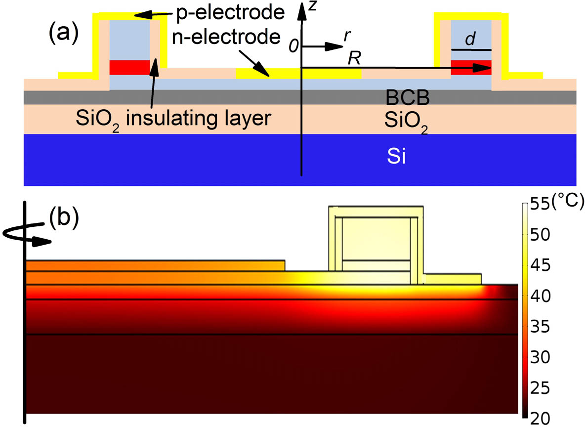
Fig. 1. (a) 2D structures used in the thermal simulation. (b) 2D temperature distributions at dissipated power of 20 mW for the hybrid microring lasers with the radius R = 20 μm d = 3.5 μm
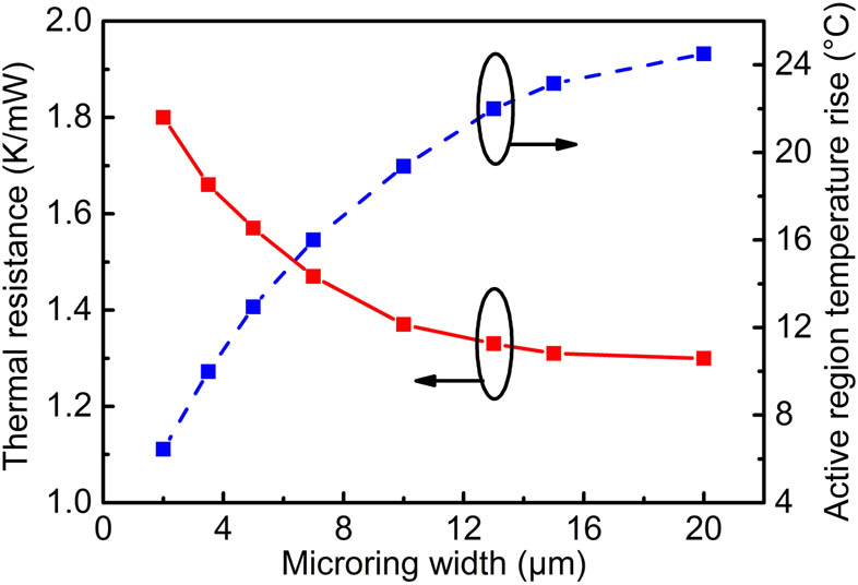
Fig. 2. Thermal resistance I th Δ T 1 kA / cm 2 d
Fig. 3. (a) Calculated threshold current I th R d I th d R = 20 μm
Fig. 4. Calculated threshold current versus the stage temperature rise for microring resonators with the radius of 30 μm and the ring width of 2, 3, and 5 μm, respectively.
Fig. 5. (a) Cross-sectional view of the microring laser used in the 3D FDTD simulation. (b) Calculated output coupling efficiency η α bot h bot
Fig. 6. (a) Cross-sectional field patterns of magnetic component H z y = 0 TE 1,15 h = 50 h bot = 0 x = 1.25 μm Γ
Fig. 7. Diagrams of the fabrication steps. (a) ICP etch to the BCB layer. (b) ICP etch to inner-bottom contacting layer and SiO 2 n p
Fig. 8. (a) Top view and (b) cross-sectional view SEM images of an AlGaInAs/Si hybrid microring laser vertically coupled to a silicon waveguide.
Fig. 9. Output power and applied voltage versus CW injection currents for the hybrid microring lasers with (a) outer-bottom contacting layer and Δ = 500 nm Δ = 500 nm Δ = − 100 nm
Fig. 10. (a) Output power from the silicon waveguide and applied voltage versus CW injection current at 8°C, 20°C, 35°C, 45°C and 55°C. (b) Lasing spectra at CW injection currents of 6 and 17 mA at 20°C for a microlaser with a radius 30 μm and a ring width of 3 μm.
Fig. 11. Lasing wavelength Δ λ Δ P

Set citation alerts for the article
Please enter your email address
© Copyright 2018-2021 | Chinese Laser Press. All Rights Reserved 沪ICP备15018463号-20