Shao-Shuai Sui, Ming-Ying Tang, Yue-De Yang, Jin-Long Xiao, Yun Du, and Yong-Zhen Huang*
Abstract
Thermal characteristics are numerically investigated for the hybrid AlGaInAs/InP on silicon microring lasers with different ring radii and widths. Low threshold current and low active region temperature rise are expected for a microring laser with a narrow ring width. Based on the thermal analysis and the 3D simulation for mode characteristics, a hybrid AlGaInAs/InP on silicon microring lasers with an inner n-electrode laterally confined by the p-electrode metallic layer is fabricated using an adhesive bonding technique. A threshold current of 4 mA is achieved for a hybrid microring laser with a radius of 20 μm and a ring width of 3.5 μm at 12°C, and the corresponding threshold current density is as low as 1 kA∕cm2. The influence of the location of silicon waveguide on output performance is studied experimentally for improving the output coupling efficiency. Furthermore, continuous-wave electrically injected lasing up to 55°C is realized for a hybrid microring laser with a radius of 30 μm and a ring width of 3 μm.China under grant 2012AA012202 and NSFC/RGC joint projectunder grant 61431166003. The authors thank Professor Andrew W. Poon and the Nanoelectronics FabricationFacility (NFF) of HKUST for support in the fabrication ofsilicon waveguides.1. INTRODUCTION
Silicon photonics have attracted significant attention due to their high speed, low cost, and large data transmission capacity [1–4], and extensive researches have focused on the passive devices for on-chip optical interconnection, including filters [5], modulators [6], switches [7], and buffers [8]. However, electrically pumped light sources on silicon are most challenging due to the indirect bandgap and low light-emission efficiency for silicon [9,10]. Hybrid integration of III/V semiconductor materials on silicon through bonding technologies provides a promising way to realize low-power-consumption light sources on an Si wafer. Molecular bonding technique [11–13], divinylsiloxane-benzocyclobutene (DVS-BCB) adhesive bonding technique [14–16], and metal bonding technique [17] are applied to fabricate hybrid III–V/Si bonded lasers. Microlasers are desirable light sources for densely integrated photonics because of the low power consumption and small footprints. Hybrid microdisk lasers with a diameter of 7.5 μm and microlasers based on resonant grating cavity mirrors were demonstrated on a silicon wafer [18,19]. Low threshold hybrid microring laser side-coupled to a silicon waveguide was fabricated through e-beam lithography [20], which has the advantages of high injection efficiency and small active region volume. Recently, we have reported a 16-wavelength hybrid microdisk laser array, which is only pulsed operation due to high threshold and thermal resistance [21]. Furthermore, mode characteristics of vertically Si-waveguide-coupled hybrid microring lasers with sloped sidewalls are studied, and a 19 μm radius hybrid microring laser is fabricated with a threshold current density of by standard lithography technique [22]. However, the operation characteristics of the microlasers are greatly influenced by the thickness of the external n-InP contacting layer surrounding the microring resonator.
In this paper, the hybrid microring lasers vertically coupled to a silicon waveguide with the -electrode in the central region of the microring resonators are fabricated using the DVS-BCB bonding technique, for improving the optical confinement of the whispering gallery modes (WGMs). In Section 2, the thermal characteristics and threshold currents are analyzed for the hybrid microring lasers with different ring radii and widths, and low threshold current and low active region temperature rise are expected by reducing the ring width. In Section 3, device parameters are optimized based on the mode characteristics of the hybrid microring resonator simulated by the 3D finite-difference time-domain (FDTD) method. In Section 4, the fabrication processes of optimized hybrid microring lasers are presented. In Section 5, a continuous-wave (CW) threshold current of 4 mA is reported for a hybrid microring laser with a radius of 20 μm and a ring width of 3.5 μm at 12°C, and CW operation up to 55°C is realized for a hybrid microring laser with a radius of 30 μm and a ring width of 3 μm. Finally, the summary is given in Section 6.
2. ANALYSIS OF THERMAL CHARACTERISTICS AND THRESHOLD CURRENTS
Ignoring the underneath Si waveguide, we perform thermal simulation for the microring lasers in a 2D schematic diagram, as shown in Fig. 1(a), based on the circular symmetry. The lateral -electrode layer is used to improve the thermal conductivity of the device, where is the microring radius and is the microring width. The thermal characteristics are simulated using the finite-element method (FEM) for the microring lasers according to the heat equation, where is the mass density, is the specific heat, is the temperature distribution, is the time, and are the cylindrical coordinates, is the heat dissipation per unit volume assuming a uniform distribution in the active region, which is approximately equal to the total dissipated electric power, and is the thermal conductivity. The radiation effects and heat convection are neglected in the thermal simulation. According to the fabricated microlasers, the thicknesses of the active layer, the upper-cladding layer, lower-cladding layer, the BCB layer, the buried oxide layer, insulating layer, and -electrode layer are taken to be 300 nm, 1.2 μm, 350 nm, 400 nm, 1 μm, 400 nm, and 300 nm, respectively. The thermal conductivities are 150, 0.3, 131, 1.27, 6, and 40 W/m·K for -electrode, BCB, Si, , AlGaInAs active layer, and InP, respectively, which is described in [23]. For the hybrid microring laser with the radius of 20 μm and the width of 3.5 μm, the 2D temperature distributions are shown in Fig. 1(b) at the dissipated electric power of 20 mW and the stage temperature of 20°C. The corresponding temperature rise is 33°C in the active region. Compared with the lasers without lateral -electrode layer, the active region temperature decreases by 16°C.
Sign up for Photonics Research TOC. Get the latest issue of Photonics Research delivered right to you!Sign up now
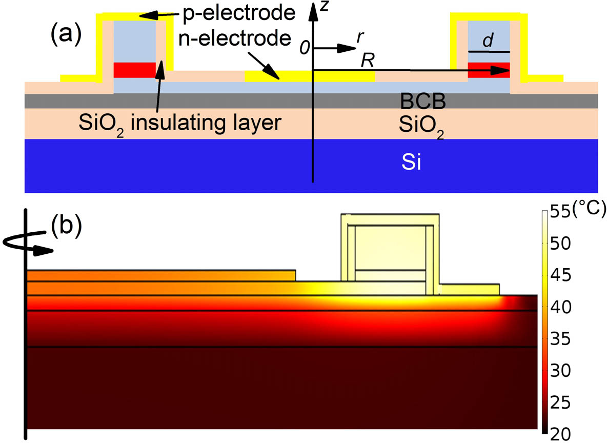
Figure 1.(a) 2D structures used in the thermal simulation. (b) 2D temperature distributions at dissipated power of 20 mW for the hybrid microring lasers with the radius and the ring width .
Thermal resistance and active region temperature rise versus the ring width are plotted in Fig. 2 for the microring lasers with the radius of 20 μm, at the injected current density of and the applied voltage of 1.5 V. As the ring width decreases from 20 to 2 μm, the thermal resistance increases from 1.3 to 1.8 K/mW, while the corresponding active region temperature rise decreases from 24°C to 6°C. Therefore, narrowing the ring width is important for improving the operation characteristics for the BCB-bonded microlasers.

Figure 2.Thermal resistance and active region temperature rise at current density of versus microring width for the 20 μm radius microlaser.
In order to elaborate on the impact of the ring width on lasing characteristics, we calculate the threshold current for the microring lasers by [20] where is the elementary electric charge; is the active region volume; is the transparent carrier density; is the quantum well optical confinement factor; is the quantum well material gain; is the injection efficiency; is the internal modal loss, , , and are defect, bimolecular, and temperature dependent Auger recombination coefficients, respectively; and is the cavity out-coupler loss with the out-coupling efficiency. The parameters , , , , , , , and are used in the simulation.
The calculated threshold currents versus the microlaser radius are plotted in Fig. 3(a) for the microlasers with different ring widths. Compared with the microring lasers, the threshold currents of the microdisk lasers increase much faster with the radius because of the relatively larger active region volume and lower injection efficiency to the lasing mode. The calculated threshold currents versus the microring width for the microlasers with a radius of 20 μm are shown in Fig. 3(b) as the circles and the squares, for the cases with and without the thermal effects, respectively. Ignoring the thermal effects, the threshold current only increases from 2.5 to 15.2 mA as increases from 2 to 20 μm. However, considering the current-induced temperature rise and the characteristic temperature , which is obtained from our hybrid microlaser under pulsed injection near room-temperature, the threshold current increases from 2.7 to 15.2 mA as increases from 2 to 7 μm, and the CW operation is not possible as due to the large temperature rise. Compared with the hybrid microdisk lasers, the microring laser with a narrow ring width laterally confined by -electrode can greatly reduce the increases of the active temperature and the threshold current, especially as the device radius increases. In a practical case, considering the fundamental mode field distribution, the threshold current will increase as due to the scattering loss induced by the imperfect sidewall of the microring resonator. For a 30-μm-radius microring laser with , Fig. 4 gives the calculated threshold currents as the functions of stage temperature rise at the ring width of 2, 3, and 5 μm. The CW operation at elevated temperature can be realized by narrowing the ring width. The maximum CW operating temperature increases by about 50°C as the ring width decreases from 5 to 2 μm, which may meet the requirement for the practical applications.
Figure 3.(a) Calculated threshold current versus microlaser radius at different ring width . (b) Threshold currents versus the microring width at , as the circles and the squares, with and without the heating effect, respectively.
Figure 4.Calculated threshold current versus the stage temperature rise for microring resonators with the radius of 30 μm and the ring width of 2, 3, and 5 μm, respectively.
3. MODE SIMULATION AND OPTIMIZATION
In this section, the mode characteristics of the transverse electric (TE) modes in a small-size microring resonator with a diameter of 3 μm and a ring width of 1.2 μm are investigated by 3D FDTD method, as shown in Fig. 5(a), due to the limited computation power of our computing system. The thicknesses of the upper-cladding layer, the active region, the insulating layer, the gold electrode layer, the BCB layer and the buried oxide layer are 1.2, 0.3, 0.25, 0.1, 0.4, and 1 μm, respectively. The silicon waveguide has a width of 500 nm and a height of 300 nm. The corresponding refractive indices of the InP layer, the active region, the BCB layer, the , the gold electrode layer, and the silicon waveguide are taken to be 3.17, 3.4, 1.54, 1.45, , and 3.48, respectively.
Figure 5.(a) Cross-sectional view of the microring laser used in the 3D FDTD simulation. (b) Calculated output coupling efficiency and scattering loss caused by outer-bottom contacting layer versus the outer-bottom contacting layer thickness .
The output coupling efficiency and the radiation loss induced by the outer-bottom contacting layer are plotted as functions of the outer-bottom contacting layer thickness in Fig. 5(b) for the vertically fundamental mode at . The radiation loss dramatically rises with as it is larger than 80 nm. In addition, decreases from 48.7% to 28.2% due to the larger radiation loss as increases from 0 to 120 nm. Therefore, the microring laser with the inner-bottom contacting layer at is important for improving the output efficiency and the threshold current.
The cross-sectional field patterns of the -directional magnetic component at plane are plotted in Fig. 6(a) for microring resonators with , 200, 350, and 500 nm and , and the corresponding normalized vertical field distributions are plotted in Fig. 6(b) at , with the optical confinement factors of 0.136, 0.184, 0.192, and 0.178. The asymmetrical distributions relative to the middle of the active region at small thickness and 200 nm will result in a large absorption loss in the heavy-doped p-InGaAs ohm contacting layer. In addition, the thick lower-cladding layer will greatly reduce the output coupling efficiency. Therefore, the optimal lower-cladding layer thickness of 350 nm is adopted in the experiment with an optical confinement factor of 0.192, and output coupling efficiency as high as 48.7% is expected as ignoring the internal absorption loss.
Figure 6.(a) Cross-sectional field patterns of magnetic component at for the vertically fundamental mode at , 200, 350, and 500 nm and . (b) Corresponding vertical normalized field amplitudes at , where is the optical confinement factor in the active layer.
4. DEVICE FABRICATION PROCESS
The hybrid microring lasers are fabricated using an AlGaInAs/InP laser wafer grown on a p-InP substrate by metal-organic chemical vapor deposition. The laser wafer comprises an InGaAsP etch-stop layer, a 0.1 μm layer as the -electrode contacting layer, a 1.1 μm p-InP cladding layer, eight compressively strained AlGaInAs quantum wells with the well thickness of 5 nm and the barrier thickness of 9 nm sandwiched between two 90 nm AlGaInAs separated confined layers, and a 0.35 μm n-InP as the lower-cladding and -electrode contacting layer.
Using DVS-BCB Cyclotene 3022-35, we bonded the laser wafer on a SOI wafer, with silicon optical waveguides formed in the SOI wafer, which has a 360 nm top silicon and a 1 μm buried oxide layer. The simple cleaning processes are performed for the SOI wafer, and the adhesion promoter solution is spin-coated on the SOI wafer to improve the adhesion of the polymer. Then, the DVS-BCB solution is spin-coated onto the SOI wafer with the BCB thickness less than 100 nm above the Si waveguide, in order to keep high coupling efficiency to the silicon waveguide. After that, the SOI wafer is baked for 15 min at 140°C to remove the solvents, and the laser wafer die at a size of is bonded on the SOI wafer. The bonded wafer is annealed at 250°C for 1 h in a atmosphere. Finally, the bonded laser wafer is slowly cooled to room temperature, and the p-InP substrate is removed by physically grinding and chemical etching processes, with a solution to remove the InP substrate and a solution to etch the InGaAsP etch-stop layer, respectively.
The fabrication processes of vertically waveguide-coupled hybrid microring lasers are summarized as follows: a 400 nm layer is first deposited on the bonded laser wafer by plasma-enhanced chemical vapor deposition. The microdisk resonator patterns are transferred onto the layer using a contact photolithography technique. The patterned layer is used as a hard mask to etch the AlGaInAs/InP wafer to the BCB bonding layer by inductively coupled plasma (ICP) etching process, as shown in Fig. 7(a). Then, a 300 nm layer is deposited on the wafer as a hard mask. The microring resonator is fabricated through the second-step ICP etch process, and a inner-bottom contacting layer inside the microring resonator is formed at the same time. After that, a 250 nm insulating layer is deposited, as illustrated in Fig. 7(b). Subsequently, an AuGeNi -electrode layer inside the microring resonator is deposited on the bottom contacting layer by electron-beam evaporation and lift-off process, as shown in Fig. 7(c). Finally, a TiPtAu -electrode layer is deposited on top of the microring resonator, as shown in Fig. 7(d).
Figure 7.Diagrams of the fabrication steps. (a) ICP etch to the BCB layer. (b) ICP etch to inner-bottom contacting layer and insulating layer deposition. (c) -electrode deposition. (d) -electrode deposition.
The top-view scanning electron microscope (SEM) image of the vertically waveguide-coupled hybrid microring laser is displayed in Fig. 8(a), and the cross-sectional-view SEM image of a hybrid microring laser is shown in Fig. 8(b). The silicon waveguide has a width of 2 μm and a height of 300 nm. The thicknesses of the BCB bonding layer above the silicon waveguide and inner-bottom contacting layer are about 80 and 300 nm, respectively.
Figure 8.(a) Top view and (b) cross-sectional view SEM images of an AlGaInAs/Si hybrid microring laser vertically coupled to a silicon waveguide.
5. OUTPUT CHARACTERISTICS OF HYBRID MICRORING LASERS
The hybrid lasers with the -side up are bonded on a thermoelectric cooler (TEC) for measurements after the hybrid laser sample is cleaved. The total output powers are measured as the sum of that from both sides of the silicon waveguide, by butt-coupling a multimode optical fiber to the cleaved silicon waveguide end face. The horizontal difference is defined as the mismatch between the III/V microring resonator and Si waveguide, as shown in the inset of Fig. 9. For , the microring resonator edge is aligned with the outer edge of Si waveguide. For , the Si waveguide is away from the microring center. The total output powers versus the CW injection current are plotted in Fig. 9 for the hybrid microring lasers with a radius of 20 μm and a ring width of 3.5 μm, at (a) and , (c) and , and (e) and , respectively, at the TEC temperature of 12°C. The CW threshold current and the threshold current density are 9.5 mA and , respectively, for the microring laser with outer-bottom contacting layer in Fig. 9(a). The corresponding total output power is 24.7 μW at 20 mA, and the lasing spectrum at 15 mA is plotted in Fig. 9(b) with the side-mode suppression ratio (SMSR) of 12.5 dB. By adopting an inner-bottom contacting layer, we have the threshold current of 4 mA, the threshold current density as low as , and the total output power of 63 μW at 20 mA in Fig. 9(c). The corresponding lasing spectrum at 15 mA is plotted in Fig. 9(d) with the main lasing mode wavelength of 1591.75 nm and the SMSR up to 28.4 dB. Furthermore, the output coupling efficiency is improved by adjusting the position of the silicon waveguide at , and an optimum range from to 200 nm is expected to achieve high output coupling efficiency, considering the larger coupling region and overlap between mode field in the III/V microring and silicon waveguide. The threshold current is 5.5 mA, and the total output power is 98 μW, as shown in Fig. 9(e), and the corresponding lasing spectrum in Fig. 9(f) at 15 mA has the SMSR of 27.5 dB. The results indicate that the microring laser with the outer-bottom contacting layer has higher threshold current and lower output power due to the low-mode-quality factor caused by the large radiation loss of the outer-bottom contacting layer.
Figure 9.Output power and applied voltage versus CW injection currents for the hybrid microring lasers with (a) outer-bottom contacting layer and , (c) inner-bottom contacting layer and , and (e) inner-bottom contacting layer and . (b), (d), and (f) show the corresponding lasing spectra at 15 mA, respectively. Microring radius is 20 μm; ring width is 3.5 μm.
For an AlGaInAs/Si microring laser with the radius of 30 μm and the ring width of 3 μm, the total output powers versus CW injection currents are shown in Fig. 10(a) at the TEC temperatures of 8°C, 20°C, 35°C, 45°C, and 55°C, with the corresponding threshold currents of 5, 6, 10, 14, and 18 mA. The corresponding threshold current density is at 20°C, which is lower than that of in [20]. The maximum output powers are 82.4 and 3.5 μW at the TEC temperatures of 8 and 55°C, respectively. A series resistance of 63 Ω around the threshold is estimated from the voltage-current curve at the TEC temperature of 20°C in Fig. 10(a). The lasing spectra at CW injection currents of 6 and 17 mA are measured and plotted in Fig. 10(b) at a TEC temperature of 20°C. Three sets of modes are observed corresponding to the fundamental, first-, and second-order transverse modes, respectively. The longitudinal mode interval is 3.8 nm at 1590 nm for the fundamental transverse modes, and the corresponding group refractive index is 3.53. A thermal-induced mode wavelength shift of 2.5 nm is observed from 6 to 17 mA. The mode wavelength shift versus the dissipated power is 0.095 nm/mW based on the applied power. Considering the mode wavelength redshift rate of 0.1 nm/K, we expect a temperature rise of 25 K and a thermal resistance of 0.95 K/mW. The measured lasing wavelength shifts versus the applied injection powers are shown in Fig. 11 for the microring lasers with and , and and , respectively. The lasing wavelength shifts are 1.79 and 3.44 nm at the dissipated power of 20 mW with the corresponding resonator temperature rise of 18°C and 34°C, respectively, which fits well with the simulated results in Fig. 1(b).
Figure 10.(a) Output power from the silicon waveguide and applied voltage versus CW injection current at 8°C, 20°C, 35°C, 45°C and 55°C. (b) Lasing spectra at CW injection currents of 6 and 17 mA at 20°C for a microlaser with a radius 30 μm and a ring width of 3 μm.
Figure 11.Lasing wavelength shift versus the injection power increment for the microring lasers with the radius of 20 and 30 μm, and the corresponding ring width of 3.5 and 3 μm.
6. CONCLUSIONS
In conclusion, we have demonstrated vertically waveguide-coupled hybrid silicon AlGaInAs/InP microring lasers through the DVS-BCB adhesive bonding technique. Thermal characteristics and threshold current are analyzed for microring lasers with different ring widths. Low threshold currents and elevated operation temperature are expected by reducing the ring width for the microring lasers with laterally confined -electrode layer. By optimizing the device design, a low threshold current of 4 mA is achieved for the microring laser with a radius of 20 μm and ring width of 3.5 μm at 12°C, and CW operation up to 55°C is realized for the hybrid microring laser with a radius of 30 μm and ring width of 3 μm. Furthermore, the coupling output efficiency is improved by adjusting the position of the silicon waveguide.
ACKNOWLEDGMENT
Acknowledgment. This work was supported by the High Technology Project of China under grant 2012AA012202 and NSFC/RGC joint project under grant 61431166003. The authors thank Professor Andrew W. Poon and the Nanoelectronics Fabrication Facility (NFF) of HKUST for support in the fabrication of silicon waveguides.
References
[1] M. J. R. Heck, H.-W. Chen, A. W. Fang, B. R. Koch, D. Liang, H. Park, M. N. Sysak, J. E. Bowers. Hybrid silicon photonics for optical interconnects. IEEE J. Sel. Top. Quantum Electron., 17, 333-346(2011).
[2] T. Shimizu, N. Hatori, M. Okano, M. Ishizaka, Y. Urino, T. Yamamoto, M. Mori, T. Nakamura, Y. Arakawa. Multichannel and high density hybrid integrated light source with a laser diode array on a silicon optical waveguide platform for interchip optical interconnection. Photon. Res., 2, A19-A24(2014).
[3] D. A. B. Miller. Device requirements for optical interconnects to silicon chips. Proc. IEEE, 97, 1166-1185(2009).
[4] K. Ohira, K. Kobayashi, N. Iizuka, H. Yoshida, M. Ezaki, H. Uemura, A. Kojima, K. Nakamura, H. Furuyama, H. Shibata. On-chip optical interconnection by using integrated III–V laser diode and photodetector with silicon waveguide. Opt. Express, 18, 15440-15447(2010).
[5] P. Dong, W. Qian, H. Liang, R. Shafiiha, D. Feng, G. Li, J. E. Cunningham, A. V. Krishnamoorthy, M. Asghari. Thermally tunable silicon racetrack resonators with ultralow tuning power. Opt. Express, 18, 20298-20304(2010).
[6] D. J. Thomson, F. Y. Gardes, Y. Hu, G. Mashanovich, M. Fournier, P. Grosse, J. M. Fedeli, G. T. Reed. High contrast 40 Gbit/s optical modulation in silicon. Opt. Express, 19, 11507-11516(2011).
[7] A. W. Poon, X. S. Luo, F. Xu, H. Chen. Cascaded microresonator-based matrix. Proc. IEEE, 97, 1216-1238(2009).
[8] F. Xia, L. Sekaric, Y. Vlasov. Ultracompact optical buffers on a silicon chip. Nat. Photonics, 1, 65-71(2007).
[9] H. M. S. Rong, R. Jones, A. S. Liu, O. Cohen, D. Hak, A. Fang, J. Michel. A continuous-wave Raman silicon laser. Nature, 433, 725-728(2005).
[10] H. Y. Liu, T. Wang, Q. Jiang, R. Hogg, F. Tutu, F. Pozzi, A. Seeds. Long-wavelength InAs/GaAs quantum-dot laser diode monolithically grown on Ge substrate. Nat. Photonics, 5, 416-419(2011).
[11] A. W. Fang, H. Park, O. Cohen, R. Jones, M. J. Paniccia, J. E. Bowers. Electrically pumped hybrid AlGaInAs-silicon evanescent laser. Opt. Express, 14, 9203-9210(2006).
[12] X. Sun, A. Zadok, M. J. Shearn, K. A. Diest, A. Ghaffari, H. A. Atwater, A. Scherer, A. Yariv. Electrically pumped hybrid evanescent Si/InGaAsP lasers. Opt. Lett., 34, 1345-1347(2009).
[13] Y. J. Zhang, H. W. Qu, H. L. Wang, S. Zhang, S. D. Ma, A. Y. Qi, Z. G. Feng, H. L. Peng, W. H. Zheng. Hybrid III–V/silicon single-mode laser with periodic microstructures. Opt. Lett., 38, 842-844(2013).
[14] G. Roelkens, D. V. Thourhout, R. Baets. Laser emission and photodetection in an InP/InGaAsP layer integrated on and coupled to a silicon-on-insulator waveguide circuit. Opt. Express, 14, 8154-8159(2006).
[15] S. S. Sui, M. Y. Tang, Y. Z. Huang, Y. D. Yang, J. L. Xiao, Y. Du. Eight-wavelength hybrid Si/AlGaInAs/InP microring laser array. Electron. Lett., 51, 506-508(2015).
[16] S. Stankovic, R. Jones, M. N. Sysak, J. M. Heck, G. Roelkens, D. Van Thourhout. Hybrid III–V/Si distributed-feedback laser based on adhesive bonding. IEEE Photon. Technol. Lett., 24, 2155-2158(2012).
[17] L. J. Yuan, L. Tao, H. Y. Yu, W. X. Chen, D. Lu, Y. P. Li, G. Z. Ran, J. Q. Pan. Hybrid InGaAsP-Si evanescent laser by selective-area metal-bonding method. IEEE Photon. Technol. Lett., 25, 1180-1183(2013).
[18] L. Liu, R. Kumar, K. Huybrechts, T. Spuesens, E.-J. Geluk, T. de Vries, P. Regreny, D. Van Thourhout, R. Baets, G. Morthier. An ultra-small, low-power, all-optical flip-flop memory on a silicon chip. Nat. Photonics, 4, 182-187(2010).
[19] Y. de Koninck, F. Raineri, A. Bazin, R. Raj, G. Roelkens, R. Baets. Experimental demonstration of a hybrid III–V-on-silicon microlaser based on resonant grating cavity mirrors. Opt. Lett., 38, 2496-2498(2013).
[20] D. Liang, M. Fiorentino, S. Srinivasan, J. E. Bowers, R. G. Beausoleil. Low threshold electrically-pumped hybrid silicon microring lasers. IEEE J. Sel. Top. Quantum Electron., 17, 1528-1533(2011).
[21] S. S. Sui, M. Y. Tang, Y. D. Yang, J. L. Xiao, Y. Du, Y. Z. Huang. Sixteen-wavelength hybrid AlGaInAs/Si microdisk laser array. IEEE J. Quantum Electron., 51, 2600108(2015).
[22] S. S. Sui, M. Y. Tang, Y. D. Yang, J. L. Xiao, Y. Du, Y. Z. Huang. Mode investigation for hybrid microring lasers with sloped sidewalls coupled to a silicon waveguide. IEEE Photon. J., 7, 6100209(2015).
[23] J. V. Campenhout, P. R. Romeo, D. V. Thourhout, C. Seassal, P. Regreny, L. D. Cioccio, J. M. Fedeli, R. Baets. Thermal characterization of electrically injected thin-film InGaAsP microdisk lasers on Si. J. Lightwave Technol., 25, 1543-1548(2007).

