1Beijing Key Laboratory for Precision Optoelectronic Measurement Instrument and Technology, School of Optics and Photonics, Beijing Institute of Technology, Beijing 100081, China
2Centre for Translational Atomaterials (CTAM), Swinburne University of Technology, Hawthorn, VIC 3122, Australia
3The Australian Research Council (ARC) Industrial Transformation Training Centre in Surface Engineering for Advanced Materials (SEAM), Swinburne University of Technology, Hawthorn, VIC 3122, Australia
Particle nanotracking (PNT) is highly desirable in lab-on-a-chip systems for flexible and convenient multiparameter measurement. An ultrathin flat lens is the preferred imaging device in such a system, with the advantage of high focusing performance and compactness. However, PNT using ultrathin flat lenses has not been demonstrated so far because PNT requires the clear knowledge of the relationship between the object and image in the imaging system. Such a relationship still remains elusive in ultrathin flat lens-based imaging systems because they operate based on diffraction rather than refraction. In this paper, we experimentally reveal the imaging relationship of a graphene metalens using nanohole arrays with micrometer spacing. The distance relationship between the object and image as well as the magnification ratio is acquired with nanometer accuracy. The measured imaging relationship agrees well with the theoretical prediction and is expected to be applicable to other ultrathin flat lenses based on the diffraction principle. By analyzing the high-resolution images from the graphene metalens using the imaging relationship, 3D trajectories of particles with high position accuracy in PNT have been achieved. The revealed imaging relationship for metalenses is essential in designing different types of integrated optical systems, including digital cameras, microfluidic devices, virtual reality devices, telescopes, and eyeglasses, and thus will find broad applications.
1. INTRODUCTION
Particle tracking analysis is a versatile technique capable of multiparameter measurement for in-depth understanding of the processes of synthesis, reaction kinetics, or specificity studies of various particles, including protein aggregates [1–4], extracellular particles [5,6], viruses, or liposomes [7,8]. It has broad applications in biology, virology, ecotoxicology, and drug delivery [9,10].
The principle of particle nanotracking (PNT) is to visualize and measure nanoparticles in suspension in the size range from tens of nanometers to a few micrometers based on the analysis of Brownian motion. The actual motion of a particle () is deduced from the motion of the particle in the image () following the relationship of , where is the magnification ratio of the imaging system. is defined by the imaging relationship of the system as , where and are the distances from the object and the image to the lens, respectively. Thus, it is of great importance to have preknowledge of the exact imaging relationship of an optical system for the PNT application. Currently, PNT systems based on bulky commercial optical microscopes are equipped with conventional refractive lenses with well-established imaging relationship , where is the focal distance of the lens. However, bulky commercial optical microscopic systems take significant space and have limited mobility with high costs, thus greatly limiting their applications.
The recent development of material science and nanofabrication technology has enabled various ultrathin flat lenses [11–16], which have revolutionized the imaging technology with the potential of developing aberration-free, high-performance, and ultracompact imaging systems. A myriad of rapid developments in nanophotonics and integrated photonic systems, as well as microfluidic devices for monitoring chemical reactions and biological processes, has been made possible, where high resolution in situ observation is vital. Undoubtedly, the ultrathin flat lens offers a great potential for achieving PNT in compact lab-on-a-chip devices with enormous benefits. However, such a system has yet to be demonstrated due to the lack of a clear imaging relationship that is essential for PNT for the newly developed ultrathin flat lens imaging system based on diffraction. The conventional imaging relationship based on the refraction theory is no longer valid in this case.
Sign up for Photonics Research TOC. Get the latest issue of Photonics Research delivered right to you!Sign up now
To enable broad applications of ultrathin flat lenses, including PNT, in this study, we experimentally measured the imaging relationship for a graphene metalens by using a spots array with nanoholes and micrometer spacing as the object, with which the object distance (), image distance (), as well as the magnification ratio (), have been well decided. The demonstrated microscopic system allows for measuring these distances with nanometer accuracy. The experimental measurements match well with the theoretical derivation based on the Rayleigh–Sommerfeld (RS) diffraction theory, thus confirming that the imaging relationship of diffractive metalenses can be generally applied to other ultrathin flat lenses [11–22] in both the microscopic and macroscopic regimes. In addition, we demonstrate the application of a graphene metalens in PNT, in which the accuracy of the imaging relationship is essential to calculate the exact positions of particles from the images. The results show the trajectories of particles can be tracked with an accuracy of 10 nm. Our work demonstrates an important application of integratable metalenses in PNT measurement. In the meantime, the revealed imaging relationship fills in the missing knowledge of imaging with a diffractive metalens, and thus will find broad applications in integrated imaging devices, such as digital cameras, microscopes, and telescopes.
2. MEASURING THE IMAGING RELATIONSHIP OF A METALENS
An imaging relationship describes the relation between the object distance (), image distance (), and the focal length () of a lens. The current imaging relationship for conventional lenses based on the refraction principle is expressed as , which is derived using geometric optics that assumes the wavelength of light is infinitely small. For ultrathin flat lenses based on diffraction instead of refraction [23], a similar form with a different factor can be obtained as [23] Therefore, when an object is placed at the focal plane of the lens (), the image will be in the other focal plane (). Under this circumstance, the magnification , which means that an inverted image with the same size as that of the object can be obtained. In addition, due to the different factor, the object and the image can be closer to the lens compared to the case of a refractive lens, resulting in a more compact system design for the diffractive metalens.
The imaging relationship is further evaluated by using the rigorous RS diffraction theory to calculate the imaging process of a graphene metalens. In the simulation, we designed a graphene metalens model [24,25] with a diameter of μ and a focal length of μ working at the wavelength of (details of the simulation model and the lens design can be found in Appendix A). Here we design the lens by using the RS diffraction theory to calculate the intensity distribution in the focal region [24]. The radius of each ring is determined by maximizing the focusing intensity and minimizing the full width at half-maximum (FWHM) in the plane of the focal spot. In this way, we are able to achieve subwavelength focusing resolution, which is very important in PNT. We consider point sources at different axial locations as the object; thus, the focal spots of the point sources can be regarded as the images. It is found that the imaging relationship generally holds in the region where the paraxial approximation is valid; namely, the distance between the point source and the lens plane is larger than the diameter of the lens () (see Appendix C, Fig. 5), which covers most of the application scenarios.
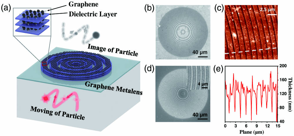
In order to experimentally verify the theoretical predictions, we designed a miniaturized lab-on-a-chip device with a graphene metalens for PNT, as shown in Fig. 1(a), where the motion of a particle is imaged by the graphene lens that is directly attached to the device. We experimentally fabricated the designed graphene metalens using femtosecond laser ablation of graphene metamaterials [25]. Such graphene metamaterials have shown unique phototunable properties and can be integrated with microfluidic devices [26]. The graphene metamaterial is prepared by using a layer-by-layer self-assembly method [26,27] with a commercial coating equipment (Innofocus, GM-AC1). The graphene metalens is fabricated by a commercial laser 3D nanoprinting setup (Innofocus Nanoprint3D). To achieve high diffraction efficiency in the focal region, Gaussian profiles for the phase and amplitude modulation functions are used to direct most of the incident light to the first diffraction order. The Gaussian profiles can be fabricated by the manufacturing laser naturally. The reflective optical microscopic image of the fabricated graphene metalens, which is composed of concentric rings of graphene metamaterials ablated by the laser, is shown in Fig. 1(b). As shown in the image, the ablated areas show lower reflectivity due to the lower refractive index of air. The atomic force microscopic (AFM) image [Fig. 1(c)] confirms the formation of air grooves in the 200 nm thick graphene metamaterial, the cross-sectional plot of which is shown in Fig. 1(e). The scanning electron microscopic (SEM) image [Fig. 1(d)] shows the linewidth of the rings is approximately 400 nm.
Figure 1.Design of the particle tracking system with a graphene metalens. (a) Schematic of the lab-on-a-chip particle tracking system with an integrated graphene metalens; inset, structure of graphene metamaterial; (b) reflective optical microscopic image of a fabricated graphene metalens; (c) atomic force microscope (AFM) image of a region of the fabricated graphene metalens; (d) SEM image of the full view and a region of the fabricated graphene metalens; (e) measured cross-sectional thickness distributions along the white dashed line in (c). Scale bars in (b) and (c) are 40 μm. Scale bar in (c) is 2.5 μm. Scale bar in the inset of (d) is 4 μm.
The imaging and focusing performances are characterized by a homemade imaging setup (see Appendix E, Fig. 7) with a commercial supercontinuum laser source (NKT Photonics, SuperK Flanium) and a CCD camera (Watec 902H). The results are analyzed using a homemade MATLAB program. The object is mounted on a 3D piezo scanning stage (Physik Instrumente) to simulate the motion of nanoparticles. The focusing capability of the graphene metalens is measured by a homemade characterization setup with a laser beam at as the incident light through a pinhole located in one of the focal planes (μ). The focal intensity distribution is magnified by through a microscopic imaging system and collected by a CCD camera [24] (the detail is in Appendix D). As expected, a high-resolution 3D focal spot can be clearly identified at the focal position of μ [see Appendix D, Figs. 6(b) and 6(c)]. The highly symmetric focal intensity distributions in the and planes [see Appendix D, Fig. 6(d)] suggest the high quality of the fabricated lens. The FWHM in the lateral direction () is and that in the axial direction () is , respectively, which confirms subwavelength resolution in the focal plane has been achieved.
In order to validate the imaging relationship of the graphene metalens, it is necessary to accurately measure the object distance () and the image distance () from the lens, which requires a well-defined object. Moreover, to measure the magnification ratio of the imaging system, the object should have known distances between different parts. To simultaneously meet all the requirements, we fabricated a scale-regulated spot array gauge with different interspot distances of 3, 5, and 7 μm on a gold thin film (200 nm thick) coated on a glass substrate using laser ablation. The diameter of the spots (nanoholes) is around 400 nm, as shown in the SEM image [Fig. 2(b)]. The spot array object is first placed in one of the focal planes of the lens [Fig. 2(a)]. As expected, a clear image shows up in the other focal plane, which confirms the derived imaging relationship as presented in Eq. (1) [23]. The optical microscopic images of the object and the resulting image from the lens are shown in Fig. 2(c), in which one can see an inverted image with almost identical intensity distributions. Furthermore, the intensity cross-sectional plots along the vertical () and horizontal () directions of the object and the image can overlap with each other nicely, suggesting high-fidelity imaging performance of the graphene metalens. The magnification ratio of the system is exactly 1, as predicted.
Figure 2.Imaging performance of the graphene metalens. (a) Schematic of imaging experiment of the spot array object imaged by the graphene metalens. (b) SEM image of the spot array object; (c) optical image of the object and image from the graphene metalens; cross-sectional intensity distribution along the (d) horizontal lines and (e) vertical lines of the spots array from the sample and image. Scale bars in (b) and (c) are 5 μm. Scale bar in the inset of (b) is 0.4 μm.
In addition, the same setup is used to measure the object and image distances from the lens to reveal the exact imaging relationship. Here we pick up one of the spots in the array shown in Fig. 2(c) as the object, which is moving along the optical axis ( axis) of the graphene metalens, and the image distance is measured by taking image stacks along the axis with a scanning stage moving at 0.1 μm step. The intensity distributions of the imaged spots in the plane are shown in Fig. 3(b), where one can see when the object is moving away from the lens, the imaging positions show an opposite trend. By comparing the experimental results with the theoretical predictions from the RS theory, we can see a good agreement, as shown in Fig. 3(c). In addition, the experimental results are fitted by Eq. (1) from the derivation with a good match, validating the imaging relationship. In this way, the imaging relationship of metalenses has been developed and characterized experimentally for the first time, we believe.
Figure 3.Imaging an object moving along the axial direction of the graphene metalens. (a) Schematic for measuring the object and image distances from the lens on the -axis; (b) measured intensity distribution in the plane with different object distances from 250 to 350 μm; the white dashed line marks the focal plane of the lens where μ. (c) Calculated and experimentally measured image distance distributions as a function of the object distance.
The imaging relationship of graphene metalenses allows its application in PNT to monitor the exact 3D motions of particles with displacement along the three axes as , , . By using the imaging relationship, we can obtain the following equation to accurately calculate by knowing the displacement of the image along the axis as : Then the magnification ratio from the motion can be worked out as . Thus, by measuring the motion of the particles in the imaging plane along the and axes as , , the exact motion of the particles in the object plane can be calculated as In this way, the 3D motion of the particles can be tracked with high accuracy, which can only be achieved by knowing the exact imaging relationship of the lens.
In order to demonstrate that different particles can be distinguished and tracked with high accuracy, an object of the Centre for Translational Atomaterials (CTAM) logo is fabricated by laser ablation, the SEM image of which is shown in Fig. 4(a). In the pattern, the circles and dots represent different types of particles. The solid shaped particles (dots) represent normal fluorescent particles, for example, fluorescent microspheres. The circles represent vortex ring-derived particles [28], which show a doughnut shape. The optical microscopic image of the object and the image from the graphene metalens are shown in Figs. 4(b) and 4(c), respectively. The image from the graphene metalens shows relatively low intensity compared to the objects due to the limited efficiency of the graphene metalens (20%). The focusing efficiency is defined as the ratio of the total power in a circular aperture with a size 3 times the FWHM of the focal spot to the total power of transmitted light through the lens [29]. In experimental measurement, we use a CCD camera to acquire the images in different planes along the axial direction. By assuming the gray scale is linearly proportional to the intensity based on the setting of gamma 1, we calculate the optical power at the lens plane within the area of the lens and the focal plane by integrating the intensity in the area. In this way, the efficiency is characterized. The efficiency can be further enhanced by introducing different modulation levels in the lens design [30]. Despite the unoptimized efficiency, the positions of the particles can be accurately measured with nanometer accuracy. The trajectories of three representative particles (marked by the red squares in Fig. 4(b), the diameters of P1, P2, and P3 are μ, μ, and μ) in the logo are studied.
Figure 4.Particle tracking analysis using the graphene metalens. (a) SEM image of the fabricated object for PNT demonstration; (b) optical microscopic image of the object; (c) image of the object from the graphene metalens (see Visualization 1); (d) trajectories of three different featured particles as a function of the number of video frames; (e), (f) lateral positions of the object and the image along the and directions in different video frames. The frame rate is 15 fps. The scale bars in (a)–(c) are 4 μm.
The object is driven by a 3D nanometer scanning stage to control the motion of the particles, which is compared to the deduced motions from the image of the graphene metalens to evaluate the position accuracy of the tracking. A movie with 15 fps (frames per second) frame rate was taken to record the process (Visualization 1). Some of the movie frames are shown in Appendix F, Fig. 8, in which one can clearly see the motion of the particles. The tracked trajectories in the plane in different time frames are plotted in Fig. 4(d). The average motions of the controlled objects and the images from the graphene metalens along the and directions are plotted in Figs. 4(e) and 4(f), respectively. Here, for easy comparison, we place the object in one of the focal planes of the graphene metalens to achieve a magnification ratio of 1. The results show the motions of the object and image are well matched with a position accuracy down to 10 nm [Figs. 4(e) and 4(f)], which confirms the feasibility and fidelity of using a graphene metalens in PNT. The same principle can be used to track particles at different positions by using the exact magnification ratio.
The position accuracy depends on a few factors. 1) The positioning accuracy of the scanning stage for holding the object. Here we used a piezo nanometer scanning stage with position accuracy down to 1 nm (Physik Instrumente), which can move the object with a well-controlled fine step. 2) Since we measured the motion of the particles by using the central position of the particle, the resolution of the graphene metalens is important to clearly resolve the particles to resolve the central position. Here, the graphene metalens has a subwavelength resolution (), which is able to resolve the particles (P1, P2, and P3), and even the doughnut-shaped ones [Fig. 4(c)]. 3) As the lens design does not consider the sine condition, the aberration, which distorts the particles, becomes serious when the particles are far from the center of the field of view (FOV) of the lens. To avoid the significant aberration affecting the position accuracy of the particles, we controlled the region of motion within the central area of the FOV. As we demonstrated previously, graphene metalenses can be integrated into a broad range of substrates and can even be used in harsh environments [26]. It is therefore promising to fabricate lab-on-a-chip microfluidic devices to achieve an on-chip PNT setup with a highly integrated graphene metalens for broad applications.
4. CONCLUSION
We have experimentally revealed the imaging relationship of metalenses. Outstanding agreements between the theoretical predictions based on geometric optics, RS diffraction theory, and the experimental results are achieved. In addition, we further demonstrate the first application of graphene metalenses in PNT, which shows the trajectories of particles can be tracked with nanometer accuracy (10 nm). Our work not only opens up the possibility of using metalenses for PNT in ultracompact systems, but also reveals the fundamental imaging relationship, which can be generally applied to any ultrathin flat lenses based on the diffraction principle. Therefore, the research findings can enable broad applications in advanced imaging systems, including digital cameras, eyeglasses, microfluidic devices for in situ optical imaging, nanophotonic chips, and aerospace.
Acknowledgment
Acknowledgment. B. J. and H. L. conceived the idea and developed the strategy of the project. X. L. and H. L. developed the theoretical model and designed the experiments. X. L. conducted the simulations and the experiments. S. W. contributed to the experimental design. G. C. contributed to the theoretical model development and programming. B. J. and Y. Z. supervised the project. All authors contributed to data analysis and paper writing.
APPENDIX A: THEORETICAL STUDY OF THE IMAGING RELATIONSHIP
Here we calculate the imaging positions of objects at different axial positions by using the RS diffraction theory. The object is an point light source on the optical axis with different distances from the graphene metalens. The image position is the focusing position of the point source. The result is shown in Fig.?5(a), where the different object positions are represented by different colours and the image positions are the peaks marked by the circles. The corresponding relationship is plotted in Fig.?5(b) (the black curve), which is compared with the analytic formula (the red curve).
Figure 5.(a) Intensity distribution of theoretical results of the graphene metalens with different object distances from 160 to 480 μm; (b) image distance as a function of object distance with RS simulation model and analytical formula.
We have measured the complex refractive index (including the refractive index and extinction coefficient) of the graphene multilayer material in our previous work [26]. The refractive index and the extinction coefficient are 2.02 and 0.91 at the wavelength of 600?nm. Because the lens is fabricated by laser ablation of graphene multilayer material, the lens is composed of regions of graphene multilayer materials and air. Thus, the phase contrast can be expressed as where is the thickness of the graphene metamaterial and is the wavelength of the incident light. is the refractive index. In the meantime, the amplitude contrast is where is the extinction coefficient. Here we design the lens by using the RS diffraction theory to calculate the intensity distribution in the focal region [24]; then the radius of each ring is determined by maximizing the focusing intensity and minimizing FWHM in the plane of the focal spot. In this way, we are able to achieve a subwavelength focusing resolution, which is very important in PNT. The detailed structural parameters of the graphene metalens are shown in Table?1. Our design is different from Fresnel zone plate in the following aspects. 1) The width of the rings is fixed, while the one in the Fresnel zone plate is varied according to the radius of the ring. 2) The Fresnel zone plate is designed based on paraxial approximation, which is not suitable for high numerical aperture (NA) lens design.
APPENDIX C: RS DIFFRACTION THEORY
The field distribution in focal region of the metalens can be calculated using the RS diffraction theory: where is the wave vector, and is the wavelength of the incident beam in vacuum. When a point source impinges on the graphene metalens, the wavefront can be regarded as spherical wave. The wavefront can be written as The modulated -field becomes We used MATLAB to calculate focal positions from Eqs.?(C1)–(C5) directly. Figure?5(a) shows the simulation intensity distribution along the axial direction with different object distances from 160 to 480?μm. The image distance as a function of object distance is plotted in Fig.?5(b), which agrees well with the analytical formula [Eq.?(C1) in the paper]. We note that the difference becomes larger when the object is very close to the lens (, the diameter of the metalens) because the formula was derived based on paraxial approximation, which covers numerous application scenarios of metalenses.
APPENDIX D: FOCUSING CHARACTERIZATION OF THE GRAPHENE METALENS (Fig.?6)
The focusing performance of the graphene metalens is characterized by focusing the light from a point light source which is located at one of the focal point of the lens. The corresponding focal spot is at the other focal point [Fig.?6(a)]. The corresponding intensity distributions and the cross-sectional plots are shown in Figs.?6(d)–(g). The reconstructed 3D focal spot is shown in Fig.?6(c).
Figure 6.(a) Schematic of the focusing characterization of the graphene flat lens; (b) simulated focal intensity distribution along the optical axis; (c) intensity distribution of the 3D focal spot of the graphene flat lens; experimentally measured intensity distributions in the (d) lateral and (e) axial planes; cross-sectional intensity distributions along the white dashed lines in the (f) lateral and (g) axial planes.
APPENDIX E: EXPERIMENTAL SETUP FOR IMAGING CHARACTERIZATION (Fig.?7)
The optical setup for imaging the sample is shown in Fig.?7, in which, the image from the graphene metalens is magnified by a 4f imaging system composing of an objective lens (OBJ) and a lens, and collected by the CCD.
Figure 7.Schematic diagram of the experimental setup used for imaging with the graphene metalens. The laser beam is a supercontinuum laser filtered by a narrowband filter (600 nm with bandwidth of 40 nm). The target was placed at the focal plane of the graphene metalens with the laser illumination. The Mitutoyo objective ( magnification; NA, 0.8) was used for providing more intensive illumination on the target. A tube lens with focal length of (Thorlabs, TTL150-A) was selectively used to form an image on the CCD camera. The object is mounted on a 3D scanning stage.
APPENDIX F: APPLICATION OF GRAPHENE METALENS IN PNT (Fig.?8)
The imaging frames from the recorded video, indicated by the numbers, are shown in Fig.?8. The tracked particle from the object is marked by the red square, and the corresponding particle from the image is marked by the yellow square. The trajectory of the motion is shown by the red dashed lines. As one can see, the motion shown in the image is identical to the motion shown in the object.
Figure 8.PNT movie frames. The images of the object and image from the graphene lens of the CTAM logo are recorded by the CCD with the number of frames marked in the figure. The pictures of image from the graphene metalens are flipped by 180° for easy comparison (see Visualization 1). The red and yellow dashed lines are used to mark the trajectories of the object and image. The frame rate is 15 fps.