Abstract
The low modulation bandwidth of deep-ultraviolet (UV) light sources is considered as the main reason limiting the data transmission rate of deep-UV communications. Here, we present high-bandwidth III-nitride micro-light-emitting diodes (μLEDs) emitting in the UV-C region and their applications in deep-UV communication systems. The fabricated UV-C μLEDs with emission area produce an optical power of 196 μW at the current density. The measured 3 dB modulation bandwidth of these μLEDs initially increases linearly with the driving current density and then saturates as 438 MHz at a current density of , which is limited by the cutoff frequency of the commercial avalanche photodiode used for the measurement. A deep-UV communication system is further demonstrated. By using the UV-C μLED, up to 800 Mbps and 1.1 Gbps data transmission rates at bit error ratio of are achieved assuming on-off keying and orthogonal frequency-division multiplexing modulation schemes, respectively.1. INTRODUCTION
Deep-ultraviolet (UV) communications have gained great interest recently due to a number of advantages compared with visible light communications. It is well known that solar radiation has a strong influence on visible-light-based optical communication links due to the high background noise [1]. However, most of the solar UV radiation, especially in the UV-C band between 200 and 280 nm, is absorbed by the ozone layer in Earth’s stratosphere. This results in negligible deep-UV radiation at ground level [2]. Therefore, the background noise is negligibly low for both indoor and outdoor deep-UV optical wireless communications [3]. Meanwhile, due to the strong scattering of deep-UV light in the air [4], a non-line-of-sight (NLOS) communication link, which has reduced pointing, acquisition, and tracking requirements, can be constructed by using deep-UV light sources [5]. Furthermore, due to the strong UV absorption by the ozone layer as mentioned, deep-UV communication links between satellites would be hardly traceable at ground level. Therefore, deep-UV communications in outer space are highly secure. Recently, many research efforts concentrated on deep-UV communications have been motivated by the fast development of deep-UV light sources, filters [6], and detectors [6,7]. However, the reported data transmission rates of the deep-UV communications are still quite low [6–9], and, to the best of our knowledge, the highest reported data transmission rate at a bit error ratio (BER) of so far is 71 Mbps [10]. This is mainly caused by the low modulation bandwidth of the deep-UV light sources used in the systems. In early works, deep-UV flash tubes or lamps were used. These light sources have very low modulation bandwidths, typically less than 40 kHz [8]. Recently, semiconductor UV light-emitting diodes (LEDs) have been used for deep-UV communications [3,10]. Compared with UV flashtubes or lamps, the modulation bandwidth of UV LEDs is much higher. A deep-UV LED with a modulation bandwidth of 153 MHz was reported recently [3]. However, conventional LEDs have a large chip size, typically in the millimeter range, which leads to a large resistance-capacitance (RC) time constant and thus limits the further increase in modulation bandwidth [11]. In order to achieve deep-UV communications with much higher data transmission rates, it is of paramount importance to develop novel deep-UV light sources with high modulation bandwidths.
Micro-LEDs (μLEDs), of edge dimension/diameter typically in the 10–100 μm range, have many inherent advantages for visible light communication applications [12]. Thanks to their small junction areas, μLEDs present a small capacitance [13]. Thus, compared with conventional broad-area LEDs, the modulation bandwidth of μLEDs is mainly dominated by differential carrier lifetime rather than the RC time constant [14]. Furthermore, μLEDs can be driven at very high current densities, which leads to a short differential carrier lifetime and thus a high modulation bandwidth [13]. Therefore, μLEDs are highly suitable light sources for high-speed optical communications. In our recent work, an over 800 MHz 6 dB electrical modulation bandwidth was achieved for polar μLEDs [15]. Moreover, by using a non-polar μLED, an over 1 GHz 3 dB electrical modulation bandwidth has also been reported [16,17]. By using a single visible μLED as a transmitter, a 7.91 Gbps data transmission rate was achieved at the BER of with orthogonal frequency division multiplexing (OFDM) modulation schemes [18]. However, to the best of our knowledge, deep-UV μLEDs and their applications in free-space optical communication have not yet been demonstrated.
In this paper, we present a III-nitride μLED device emitting at 262 nm and characterize its performance for the deep-UV communications. At a current density of in direct-current (DC) operation, the optical power of this deep-UV μLED is over 190 μW, corresponding to an optical power density of . The measured 3 dB electrical modulation bandwidth of this μLED is over 400 MHz at a driving current density of , which is 3 times higher than the reported bandwidth of deep-UV LEDs. By using this high-bandwidth μLED as a deep-UV light source, a deep-UV communication system is established. Up to 800 Mbps and 1.1 Gbps error-free data transmission rates at a BER of are achieved assuming on-off keying (OOK) and OFDM modulation schemes, respectively. To the best of our knowledge, these data transmission rates are more than 15 times higher than the reported results at the same BER value in the deep-UV wavelength band [10], which demonstrates the great potential of μLEDs for deep-UV communications.
Sign up for Photonics Research TOC. Get the latest issue of Photonics Research delivered right to you!Sign up now
2. UV-C μLEDS
A. Design and Fabrication of the UV-C μLED Array
A commercial AlGaN-based LED wafer grown on a c-plane sapphire substrate with a 262 nm emission wavelength was used in this work for μLED fabrication. The epitaxial structure of this wafer includes a 2 μm thick AlN buffer layer, a 2 μm thick n-doped layer, an active region consisting of six-period AlGaN-based quantum wells (QWs) with a 2.5 nm thick well and 13 nm thick barrier, a 50 nm thick electron blocking layer (EBL), and finally a 310 nm thick p-doped GaN layer. The Al compositions in the wells and barriers are estimated as 45% and 55%, respectively. The μLEDs were fabricated in a “concentric cluster” array format. The design and fabrication process of the μLED array presented in this work were similar to those reported in our previous work [15,18,19]. This μLED array consists of 15 μLEDs in a flip-chip configuration, each of trapezoidal shape with an emission area of . This area is equivalent to a disk-shape μLED with a diameter of 27 μm. With a shared cathode, each μLED is individually addressed by its corresponding anode. Figure 1 illustrates the cross-sectional schematic of a single UV-C μLED fabricated in this work. As shown, in order to reduce the capacitance and thus increase the modulation bandwidths of the μLEDs, the μLED structure was created by two -based inductively coupled plasma (ICP) etching processes. First, 15 μLEDs were defined by ICP etching, which terminated at the -type AlGaN layer. Then, an -type AlGaN mesa was created by further ICP etching down to the sapphire substrate. An annealed Pd layer with a thickness of 100 nm was used as the quasi-ohmic p-type metal contact to -type GaN [11]. A metal bilayer of Ti/Au (50 nm/300 nm) was used as the -type contact and metal tracks to connect the μLEDs. Figure 2(a) shows the optical image of the fabricated UV-C μLED array presented in this work. A high-magnification image of the μLEDs is shown in Fig. 2(b). During this work, all the measurements were performed on bare, unpackaged μLED die.
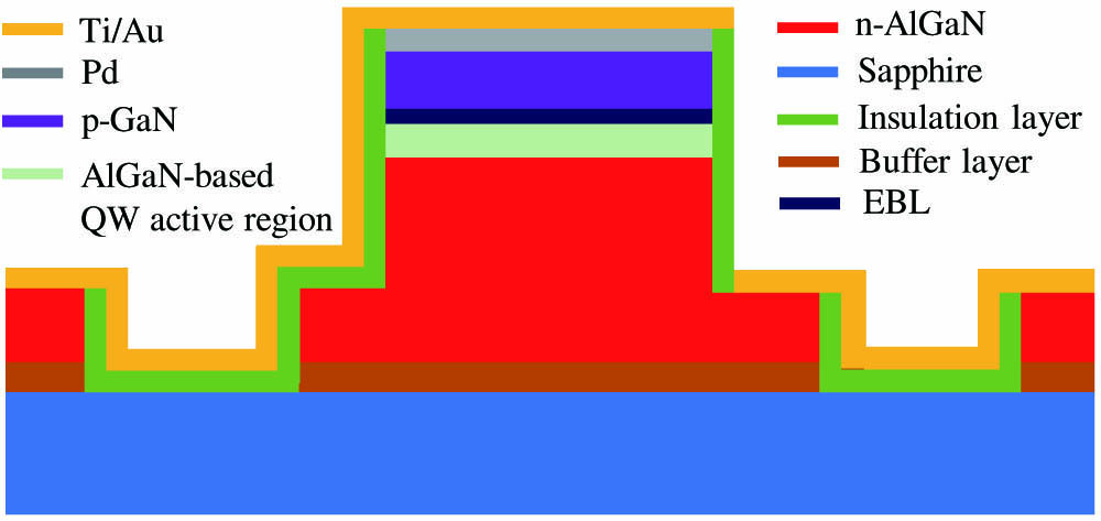
Figure 1.Simplified cross-sectional schematic of a single UV-C μLED presented in this work. Dimensions are not to scale.

Figure 2.(a) Plan view optical image of the fabricated UV-C μLED array presented in this work and (b) a high-magnification image of the μLEDs.
B. Electrical, Optical, and Modulation Bandwidth Characteristics of the UV-C μLEDs
Figure 3 presents the typical current density–voltage () and optical power–current density () curves of a single UV-C μLED from the fabricated μLED array. The inset in Fig. 3 presents the emission spectrum of the UV-C μLED at . The and data were measured at the same time by placing a UV-enhanced Si photodetector in close proximity to the polished sapphire substrate of the μLED. The curve shows that the turn-on voltage of this μLED is 13 V at (1 mA). This value is consistent with that reported in previous work on broad-area UV-C LEDs [20]. For this UV-C μLED, the high turn-on voltage is mainly attributed to the high contact resistivity of metal contact to the -type layer. A 60% Al composition in this n-type results in difficulty to achieve high-quality ohmic contact [21]. In order to reduce the turn-on voltage, we are currently working on optimizing the metal contact to the -type layer by testing different metal schemes and annealing processes. Furthermore, this μLED can be driven at a current density up to before thermal rollover. This maximum current density is much higher than the current densities () that conventional deep-UV LEDs can sustain [22]. At this current density, the unidirectional optical power output of the μLED is 196 μW at the sapphire substrate surface, corresponding to an optical power density of .
Figure 3. and characteristics of a UV-C μLED. The inset shows the emission spectrum of a UV-C μLED at .
As mentioned above, the modulation bandwidth of μLEDs is mainly dominated by the differential carrier lifetime rather than the RC time constant. The differential carrier lifetime is reduced when the operating current density increases, and compared with conventional LEDs, the operating current density of μLEDs is much higher. Therefore, a high modulation bandwidth is expected for the UV-C μLEDs fabricated in this work. To verify this, the frequency responses of these UV-C μLEDs were measured following a similar method to that described in our previous work [18]. An alternating current frequency sweep signal from a network analyzer was combined with a DC-bias current in a bias tee (SHF BT45-D) and then sent to modulate the μLED. The optical response from the μLED was first collected by two UV-enhanced optical lenses and then focused by a UV-enhanced objective lens into a UV-enhanced Si avalanche photodiode (APD) detector [Thorlabs APD430A2(/M)] with a specified output 3 dB electrical bandwidth between DC to 400 MHz. The received response was then fed to the network analyzer. Figure 4(a) shows the measured 3 dB electrical modulation bandwidth of the UV-C μLED as a function of current density. As shown, the measured modulation bandwidth increases linearly with increasing current density from 18 to , which is consistent with the relationship between the modulation bandwidth and current density we observed in our early work on visible μLEDs [12]. However, by further increasing the current density, the measured modulation bandwidth becomes saturated at around 438 MHz with a slight variation (less than 2 MHz). In order to explain this saturation, we compared the measured frequency responses of the μLED at different current densities. The typical frequency responses at [highlighted by the red circle in Fig. 4(a)] and [highlighted by the blue circle in Fig. 4(a)] are presented in Figs. 4(b) and 4(c), respectively. Compared with the frequency response at , the one at shows a sharp drop when increasing the modulation frequency to around 450 MHz. It is noticed that the APD detector used for the measurement has the similar frequency response characteristic [23]. This indicates that the observed saturation of the measured modulation bandwidth is actually caused by the APD rather than the μLED itself [24,25]. Therefore, the modulation bandwidth of the μLED fabricated in this work is expected to be much higher than 438 MHz. We have tried to repeat similar measurements using a large-bandwidth (2 GHz) deep-UV PIN detector. However, due to the low sensitivity of the detector and low optical power of the UV-C μLED, no useful signal was detected. In order to overcome these issues, the performances of both APD and deep-UV LEDs need to be further improved. Nevertheless, we emphasize that the UV-C μLED has a measured 3 dB electrical modulation bandwidth of 438 MHz at . This value is already around 3 times higher than the reported 3 dB electrical modulation bandwidth of 153 MHz [3]. Moreover, compared with our previous work based on visible c-plane μLEDs, this UV-C μLED also presents a much larger modulation bandwidth, even at low current densities. As mentioned above, the modulation bandwidths of μLEDs are dominated by their differential carrier lifetime, which is the combination of radiative and non-radiative recombination lifetimes [13]. It is well known that the quality of the AlGaN-based deep-UV LED wafer is relatively low due to the high-density defects generated in the material growth process [26]. This results in a shorter non-radiative recombination lifetime for UV-C μLEDs and thus large modulation bandwidth.
Figure 4.(a) The 3 dB electrical modulation bandwidth of the UV-C μLED as a function of current density; small signal frequency responses of the UV-C μLED at (b) 18 and (c) .
3. DEEP-UV COMMUNICATIONS USING THE UV-C μLED LIGHT SOURCE
By using the fabricated UV-C μLED as a light source, a deep-UV wireless communication system was implemented. In order to fully demonstrate the capability of this μLED for deep-UV communications, single-carrier OOK and multi-carrier OFDM modulation schemes were both used in our experiments. Figure 5 shows a schematic diagram and optical image of the setup used in this work. Both the OOK and OFDM waveforms generated in MATLAB were mapped to analog signals through an arbitrary waveform generator (AWG; Keysight 81180B). These analog signals from the AWG were then amplified by an amplifier (ZHL-6A-S+). Afterwards, the amplified analog signals and a DC bias current were combined by the bias tee and then applied to a UV-C μLED using a high-speed micro-probe. In order to optimize system performance, extensive tests were performed to determine the modulation signal depths () and DC bias current densities () used in the experiments. For the OOK modulation scheme, the and were set as 2 V and . For the OFDM modulation scheme, the and were set as 7 V and . The light emitted from the μLED was collected and focused into the UV-enhanced Si APD detector by a UV-enhanced lens. The distance between the μLED and the APD detector was around 0.3 m. In this setup, a combination of light scattering and non-optimized collection optics and optical alignment results in only 20% of the emitted light power being received by the APD. This means that around 26 μW and 30 μW optical power were illuminated onto the APD detector for the OOK and OFDM modulation schemes, respectively. Improvement to this system is ongoing. The output signal of the APD detector was fed into a digital oscilloscope (Keysight, MSO7104B) and processed offline in MATLAB.
Figure 5.Schematic diagram and optical image of the experimental setup for deep-UV communication using the fabricated UV-C μLED.
A. OOK Modulation Scheme
For the OOK modulation scheme, two information symbols were first mapped to different amplitudes and then further referred to as transmitted symbols. Non-return-to-zero (NRZ) symbols are used, and the set of transmitted symbols is . A root raised cosine filter was used before the transmitted symbols were sent to the AWG. To obtain the received symbol, the received signal was filtered by a matched filter and down-sampled. Figure 6(a) illustrates the normalized number of occurrences of transmitted and received symbols of OOK represented by histograms at 800 Mbps. As shown, the distribution of symbols generated at the transmitter (black parts) is uniform, but that of received symbols before the equalizer (blue parts) is negative-side heavier. This is mainly due to the so-called intersymbol interference (ISI) [27], which is caused by the amplitude and delay distortions from the communication channel. In order to mitigate this phenomenon, a feedforward equalizer based on the recursive least-squares updating algorithm was deployed. This equalizer estimates the received symbols that go beyond a decision threshold and then decodes them to their nearest transmitted symbols. As presented by the brown data in Fig. 6(a), after the equalization, the spread of received symbols becomes narrow, which leads to a lower BER. This reduces the decoding errors due to the ability to distinguish the correctly transmitted symbols at the receiver. Figure 6(b) shows the eye diagram of the received signal assuming the OOK modulation scheme at 800 Mbps after equalization. As shown, the open eyes can be clearly distinguished, demonstrating a communication link with a low BER. Higher data transmission rates cannot be measured due to the limitation from the bandwidth of the APD detector.
Figure 6.(a) Normalized number of occurrences of transmitted and received symbols assuming the OOK modulation scheme at 800 Mbps and (b) the eye diagram of received symbols assuming the same measurement conditions using the UV-C μLED.
B. OFDM Modulation Scheme
The influence of ISI on the BER in a single-carrier modulation scheme such as OOK would become more pronounced with the increase of the data transmission rate. As a result, the equalizer would be more computationally complex for high-speed communications [18]. A cost-effective way to simplify the equalizer is to apply OFDM with a single tap equalizer. The encoding method of the OFDM is done by modulating binary bits into -ary quadrature amplitude modulation (-QAM) symbols, where is the constellation order. Then, depending on the available signal-to-noise ratio (SNR), different constellation sizes are loaded on the subcarriers using the adaptive bit and energy loading. An inverse fast Fourier transformation (IFFT) is used to multiplex QAM symbols into subcarriers. By introducing Hermitian symmetry on the OFDM frame, a real-valued output is guaranteed. With the purpose of shifting the negative OFDM samples to positive, a DC bias is imposed. The details of this method can be found in our early work [18]. In this measurement, the sampling frequency of the AWG is 4 GS/s, and the oversampling factor of the root raised cosine is set as 4. Fast Fourier transformation (FFT) is applied on the received signal, and the received QAM symbols are equalized using the estimated channel. Figure 7(a) shows the measured SNR versus bandwidth of a UV-C μLED at and , and the recovered -QAM constellations for , 8, 16 are inserted as well. The SNR performance of at least 5 dB is shown up to 480 MHz of bandwidth. This value is good enough for the decoder to distinguish the transmitted symbols from -QAM constellations for , 8, 16, which enables high-speed deep-UV communication. Figure 7(b) presents the measured data transmission rates versus BER using the OFDM modulation scheme. Up to 1.1 Gbps data transmission rate is achieved at the BER of . In Table 1, we compared our deep-UV communication results with those from other published work. As listed, on the other hand, thanks to the high-bandwidth character of the used UV-C μLED, we achieved the highest data transmission rate at the BER of under the strong limitation from the APD detector used. Although the transmission distance of our work is strongly limited by the optical power produced from the UV-C μLED, this low optical power minimizes the adverse effects of UV radiation in communications.
Figure 7.(a) Measured SNR versus bandwidth for OFDM at and . -QAM constellation symbols received at the photodetector after equalization for , 8, 16 are inserted. (b) Data transmission rate versus BER for OFDM measurement at and .
| Light Source | Modulation Scheme | Transmission Power | Channel Length | Data Rate | BER | Ref. |
| 265 nm mercury-xenon lamp | PPM | 25 W | 1.6 km | 1.2 Mbps | – | [8] |
| 253 nm mercury-argon lamp | PPM | 5 W | 0.5 km | 10 kbps | 10−5 | [9] |
| 254 nm low-pressure mercury lamp | FSK | – | 6 m | 1.2 kbps | 10−4 | [6] |
| 265 nm LED arrays | OOK/PPM | 43 mW | 10 m | 2.4 kbps | 10−4 | [7] |
| 294 nm LED | OFDM | 190 μW | 0.08 m | 71 Mbps | 3.8×10⁻³ | [10] |
| 280 nm LED | PAM-4 | – | 1.5 m | 1.6 Gbps | 2.0×10⁻² | [3] |
| 262 nm μLED | OFDM | 196 μW | 0.3 m | 1.1 Gbps | 3.8×10⁻³ | This work |
Table 1. Comparison of Deep-UV Communication Results from the Literature, and from This Work
4. CONCLUSION
The design, fabrication, and performance of III-nitride UV-C μLEDs are presented in this paper. Each UV-C μLED could be operated at a DC current density up to with a directed optical power up to 196 μW. Due to the limitation of the commercial APD detector used in this work, the maximum measured 3 dB electrical modulation bandwidth of the UV-C μLED linearly increased in a small current density range and saturated at 438 MHz at a current density of . This modulation bandwidth is 3 times higher than the reported bandwidth of conventional deep-UV LEDs. The UV-C μLED was further used as the light source in a free-space deep-UV communication system. Thanks to its high-bandwidth character, up to 800 Mbps and 1.1 Gbps data transmission rates at a BER of are achieved assuming OOK and OFDM modulation schemes, respectively. These high data transmission rates demonstrate the great potential of μLEDs for deep-UV communications.
Acknowledgment
Acknowledgment. We acknowledge Qingdao Jason Electric Co., Ltd for providing the deep-UV LED materials. The data is available online at https://doi.org/10.15129/0efd3fc2-7f3d-4647-bb56-8f470d80fed4.
References
[1] M. S. Islim, S. Videv, M. Safari, E. Xie, J. J. D. McKendry, E. Gu, M. D. Dawson, H. Haas. The impact of solar irradiance on visible light communications. J. Lightwave Technol., 36, 2376-2386(2018).
[2] Z. Xu, B. M. Sadler. Ultraviolet communications: potential and state-of-the-art. IEEE Commun. Mag., 46, 67-73(2008).
[3] K. Kojima, Y. Yoshida, M. Shiraiwa, Y. Awaji, A. Kanno, N. Yamamoto, S. Chichibu. 1.6-Gbps LED-based ultraviolet communication at 280 nm in direct sunlight. European Conference on Optical Communication (ECOC), 1-3(2018).
[4] S. Karp, R. M. Gagliardi, S. E. Moran, L. B. Stotts. Optical Channels: Fibers, Clouds, Water, and the Atmosphere(2013).
[5] D. E. Sunstein. A scatter communications link at ultraviolet frequencies(1968).
[6] T. Feng, F. Xiong, Q. Ye, Z. Pan, Z. Dong, Z. Fang. Non-line-of-sight optical scattering communication based on solar-blind ultraviolet light. Proc. SPIE, 6783, 67833X(2007).
[7] D. Han, Y. Liu, K. Zhang, P. Luo, M. Zhang. Theoretical and experimental research on diversity reception technology in NLOS UV communication system. Opt. Express, 20, 15833-15842(2012).
[8] J. J. Puschell, R. Bayse. High data rate ultraviolet communication systems for the tactical battlefield. Proc. IEEE, 1, 253-267(1990).
[9] M. Geller, T. E. Keenan, D. E. Altman, R. H. Patterson. Optical non-line-of-sight covert, secure high data communication system. U.S. Patent(1985).
[10] X. Sun, Z. Zhang, A. Chaaban, T. K. Ng, C. Shen, R. Chen, J. Yan, H. Sun, X. Li, J. Wang, J. Li, M.-S. Alouini, B. S. Ooi. 71-Mbit/s ultraviolet-B LED communication link based on 8-QAM-OFDM modulation. Opt. Express, 25, 23267-23274(2017).
[11] E. Xie, M. Stonehouse, R. Ferreira, J. J. McKendry, J. Herrnsdorf, X. He, S. Rajbhandari, H. Chun, A. V. Jalajakumari, O. Almer, G. Faulkner, I. M. Watson, E. Gu, R. Henderson, D. O’Brien, M. D. Dawson. Design, fabrication, and application of GaN-based micro-LED arrays with individual addressing by N-electrodes. IEEE Photon. J., 9, 7907811(2017).
[12] S. Rajbhandari, J. J. McKendry, J. Herrnsdorf, H. Chun, G. Faulkner, H. Haas, I. M. Watson, D. O’Brien, M. D. Dawson. A review of gallium nitride LEDs for multi-gigabit-per-second visible light data communications. Semicond. Sci. Technol., 32, 023001(2017).
[13] E. F. Schubert. Light-Emitting Diodes(2006).
[14] J. J. McKendry, R. P. Green, A. Kelly, Z. Gong, B. Guilhabert, D. Massoubre, E. Gu, M. D. Dawson. High-speed visible light communications using individual pixels in a micro light-emitting diode array. IEEE Photon. Technol. Lett., 22, 1346-1348(2010).
[15] R. X. Ferreira, E. Xie, J. J. McKendry, S. Rajbhandari, H. Chun, G. Faulkner, S. Watson, A. E. Kelly, E. Gu, R. V. Penty, I. H. White, D. C. O’Brien, M. D. Dawson. High bandwidth GaN-based micro-LEDs for multi-Gb/s visible light communications. IEEE Photon. Technol. Lett., 28, 2023-2026(2016).
[16] A. Rashidi, M. Monavarian, A. Aragon, A. Rishinaramangalam, D. Feezell. GHz-bandwidth nonpolar InGaN/GaN micro-LED operating at low current density for visible-light communication. IEEE International Semiconductor Laser Conference (ISLC), 1-2(2018).
[17] A. Rashidi, M. Monavarian, A. Aragon, A. Rishinaramangalam, D. Feezell. Nonpolar m-plane InGaN/GaN micro-scale light-emitting diode with 1.5 GHz modulation bandwidth. IEEE Electron Device Lett., 39, 520-523(2018).
[18] M. S. Islim, R. X. Ferreira, X. He, E. Xie, S. Videv, S. Viola, S. Watson, N. Bamiedakis, R. V. Penty, I. H. White, A. E. Kelly, E. Gu, H. Haas, M. D. Dawson. Towards 10 Gb/s orthogonal frequency division multiplexing-based visible light communication using a GaN violet micro-LED. Photon. Res., 5, A35-A43(2017).
[19] J. J. McKendry, D. Tsonev, R. Ferreira, S. Videv, A. D. Griffiths, S. Watson, E. Gu, A. E. Kelly, H. Haas, M. D. Dawson. Gb/s single-LED OFDM-based VLC using violet and UV gallium nitride μLEDs. Summer Topicals Meeting Series (SUM), 175-176(2015).
[20] N. Maeda, M. Jo, H. Hirayama. Improving the efficiency of AlGaN deep-UV LEDs by using highly reflective Ni/Al p-type electrodes. Phys. Status Solidi A, 215, 1700435(2018).
[21] M. Kneissl. A brief review of III-nitride UV emitter technologies and their applications. III-Nitride Ultraviolet Emitters, 1-25(2016).
[22] G.-D. Hao, M. Taniguchi, N. Tamari, S.-I. Inoue. Enhanced wall-plug efficiency in AlGaN-based deep-ultraviolet light-emitting diodes with uniform current spreading p-electrode structures. J. Phys. D, 49, 235101(2016).
[23] . APD 430x operation manual.
[24] R. P. Green, J. J. McKendry, D. Massoubre, E. Gu, M. D. Dawson, A. E. Kelly. Modulation bandwidth studies of recombination processes in blue and green InGaN quantum well micro-light-emitting diodes. Appl. Phys. Lett., 102, 091103(2013).
[25] J. Cho, E. Yoon, Y. Park, W. J. Ha, J. K. Kim. Characteristics of blue and ultraviolet light-emitting diodes with current density and temperature. Electron. Mater. Lett., 6, 51-53(2010).
[26] M. Shatalov, W. Sun, A. Lunev, X. Hu, A. Dobrinsky, Y. Bilenko, J. Yang, M. Shur, R. Gaska, C. Moe, G. Garrett, M. Wraback. AlGaN deep-ultraviolet light-emitting diodes with external quantum efficiency above 10%. Appl. Phys. Express, 5, 082101(2012).
[27] J. G. Proakis. Digital Communications(1995).


