
Wanqi Ren, Kyung Rock Son, Tae Hoon Park, Vignesh Murugadoss, Tae Geun Kim. Manipulation of blue TADF top-emission OLEDs by the first-order optical cavity design: toward a highly pure blue emission and balanced charge transport[J]. Photonics Research, 2021, 9(8): 1502
- Photonics Research
- Vol. 9, Issue 8, 1502 (2021)
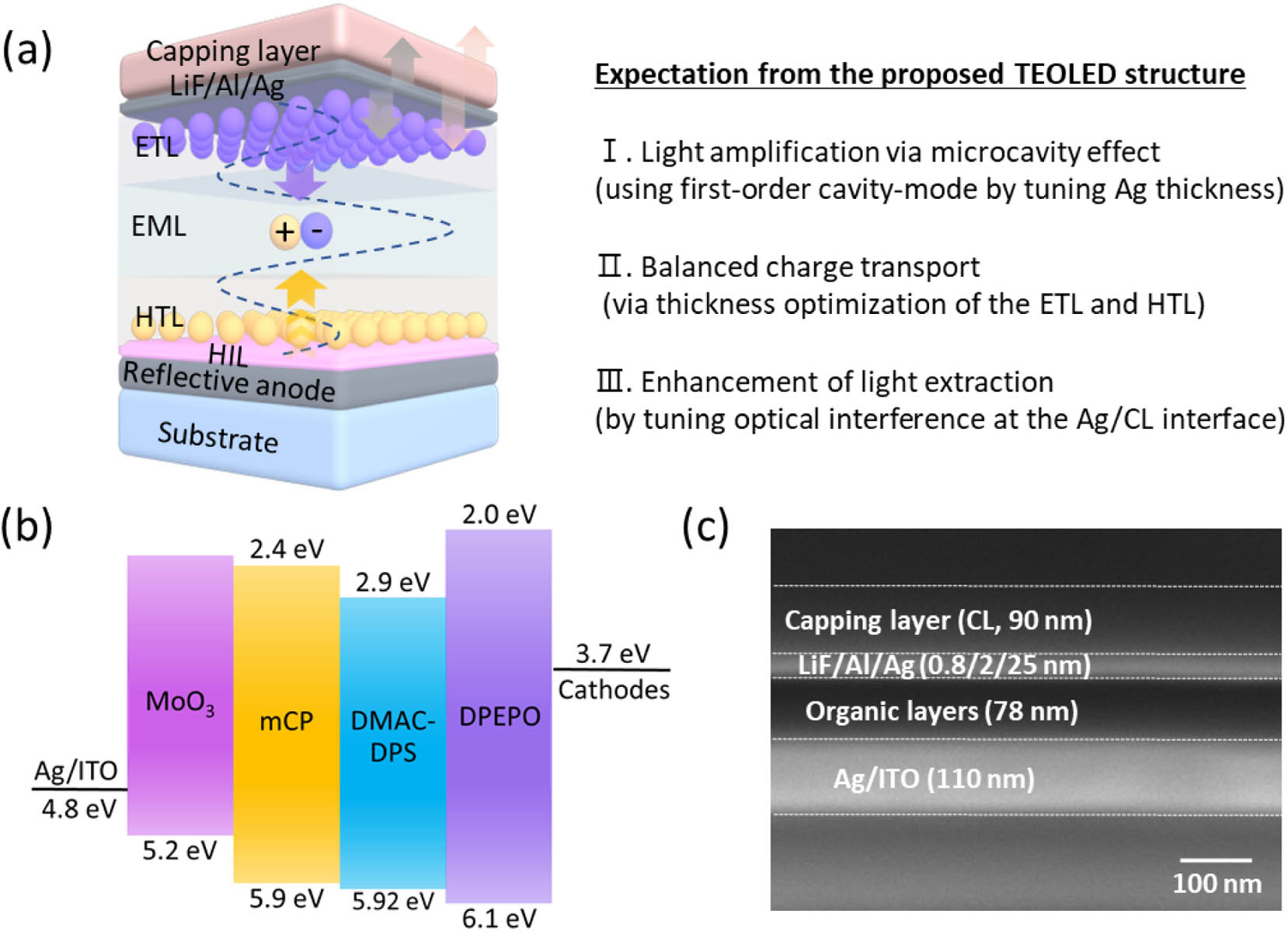
Fig. 1. (a) Schematic of the TADF TEOLED structure. (b) Diagram of HOMO and LUMO energy level for materials. (c) FIB-SEM image of the optimized device structure.
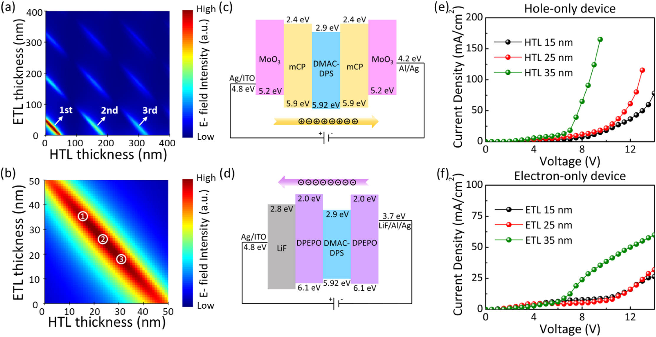
Fig. 2. (a) Simulated e-field distribution of the microcavity as a function of the HTL and ETL thickness. Each part indicated by the arrow is the thickness range of the HTL and ETL that satisfies the first-, second-, and third-order microcavity condition, respectively. (b) Simulated e-field intensity distribution of the microcavity as a function of the HTL and ETL thickness in the first-order condition (part 1: 15 nm HTL and 35 nm ETL; part 2: 25 nm HTL and 25 nm ETL; part 3: 35 nm HTL and 15 nm ETL). Schematic energy band diagrams of the (c) HOD and (d) EOD. J–V characteristics of the (e) HODs and (f) EODs with different thicknesses of HTLs and ETLs.
Fig. 3. Device performances of the TEOLEDs with different thicknesses of Ag layers: (a) J –V –L curves; (b) calibrated EQE–J characteristics; (c) CE–J characteristics; (d) EL spectra of the devices at 10 V.
Fig. 4. Schematics of optical paths in TEOLEDs (a) without and (b) with CL, and (c) simulated e-field intensity of the TEOLEDs (based on 15, 20, 25 nm Ag layers) as functions of the CL thickness and wavelength.
Fig. 5. Near-field distribution of the TEOLEDs without CL based on (a) 15 nm, (b) 20 nm, and (c) 25 nm Ag layers, and with 90 nm CL based on (d) 15 nm, (e) 20 nm, and (f) 25 nm Ag layers.
Fig. 6. Device performances of the TEOLEDs with different CL thicknesses on 25 nm Ag layer: (a) J –V –L curves; (b) calibrated EQE–J characteristics; (c) CE–J characteristics; (d) EL spectra of the devices at 10 V. (e) Viewing angle-dependent emission images captured for the tilted OLED with Ag (25 nm)/CL (90 nm) in the range from − 70 °
Fig. 7. Schematic of (a) simulation modeling and (b) refractive index information of organic materials.
Fig. 8. Simulated e-field intensity of microcavity.
Fig. 9. (a) Transmittance, (b) reflectance, and (c) absorption with respect to the sheet resistance of the LiF/Al/Ag electrode with different Ag thicknesses.
Fig. 10. Device performances of the TEOLEDs with different CL thicknesses on 15 nm Ag layer: (a) J –V –L curves; (b) calibrated EQE–J characteristics; (c) CE–J characteristics; (d) EL spectra of the devices at 10 V.
Fig. 11. Device performances of the TEOLEDs with different CL thicknesses on 20 nm Ag layer: (a) J –V –L curves; (b) calibrated EQE–J characteristics; (c) CE–J characteristics; (d) EL spectra of the devices at 10 V.
Fig. 12. EL spectra of TADF OLEDs with first-order microcavity and without microcavity at 10 V.
|
Table 1. Summary of Device Performances

Set citation alerts for the article
Please enter your email address
© Copyright 2018-2021 | Chinese Laser Press. All Rights Reserved 沪ICP备15018463号-20