
Wanqi Ren, Kyung Rock Son, Tae Hoon Park, Vignesh Murugadoss, Tae Geun Kim, "Manipulation of blue TADF top-emission OLEDs by the first-order optical cavity design: toward a highly pure blue emission and balanced charge transport," Photonics Res. 9, 1502 (2021)
- Photonics Research
- Vol. 9, Issue 8, 1502 (2021)
Abstract
1. INTRODUCTION
Thermally activated delayed fluorescence (TADF) materials are third-generation luminescent materials used instead of fluorescent and phosphorescent materials. They have attracted much attention from academia and industry [1,2] because TADF-based emitters can achieve 100% internal quantum efficiency (IQE) theoretically by reverse intersystem crossing (RISC) from the triplet excited state (
Nevertheless, the antispin process is a major factor because the material’s characteristics and the HOMO of the material are bound to change when
In this study, we present an optimized optical design and a balanced charge transport for achieving high-color-purity blue TADF TEOLEDs with a semitransparent cathode configuration. To maximize microcavity effects for the narrow emission spectra of devices (lower FWHM), the first-order cavity mode with a radiance intensity higher than that of second- or third-order cavity modes [35] was selected and carefully optimized by considering the balanced charge transport. Then, hole-only devices (HODs) and electron-only devices (EODs) were fabricated to choose the proper thickness of the carrier transport layers in order to ensure sufficient exciton recombination.
Sign up for Photonics Research TOC. Get the latest issue of Photonics Research delivered right to you!Sign up now
In addition, by tuning the optical interference near the semitransparent top cathode layers consisting of thin silver (Ag) and an organic capping layer (CL), the overall luminance efficiencies of the devices were greatly boosted, as confirmed by three-dimensional (3D) finite-difference time-domain (FDTD) simulation. We believe that highly pure blue emission can be achieved by optically and electrically optimized blue TADF TEOLEDs with thin Ag film (25 nm) and CL (90 nm) without special care for the synthesis method of TADF emitters.
2. EXPERIMENTAL DETAILS
A. Modeling
The simulated results were analyzed using commercial FDTD software (FDTD Solutions, Lumerical, Canada), and the electric field (e-field) distribution spectra were calculated based on the electrical dipole source. For the FDTD boundary conditions, we selected a perfectly matched layer (PML) as the modeling boundary condition to avoid the interference of boundary reflection on the device, thus improving the accuracy of the simulation results. In this model, the refractive indices and the coefficient indices were measured by alpha-SE ellipsometry (WizOptics, Korea).
B. Device Fabrication
Molybdenum oxide (
C. Characterization
The transmittance and reflectance spectra of the samples were measured using a UV spectrometer (PerkinElmer, Lambda 35). The current density–voltage–luminance (J–V–L), current efficiency (CE), and electroluminescence (EL) spectrum characteristics based on an effective area of
3. RESULTS AND DISCUSSION
A. Optical Design for a Pure Blue Emission and Balanced Charge Transport
The schematic of the device structure [Fig. 1(a)] shows that an optical microcavity was formed inside the device through multiple reflections of internal optical light between the top semitransparent electrode and the bottom reflective electrode to achieve optical resonance at a specific wavelength. By tuning the thickness of the HTL and ETL, the charge balance was achieved under the first-order microcavity length condition. For the cathode, a LiF/Al bilayer structure was used to reduce the electron injection barrier as well as ensure high efficiency of charge injection as shown in the energy level diagram of Fig. 1(b). The most appropriate electrode thickness of the Ag layer was chosen based on the reflectance and transmittance properties, and the effect of different CL thicknesses on the optical performance of the device was examined to maximize the light extraction via reduced microcavity effects. Our optimal structure of the device was validated by the FIB-SEM image [Fig. 1(c)].
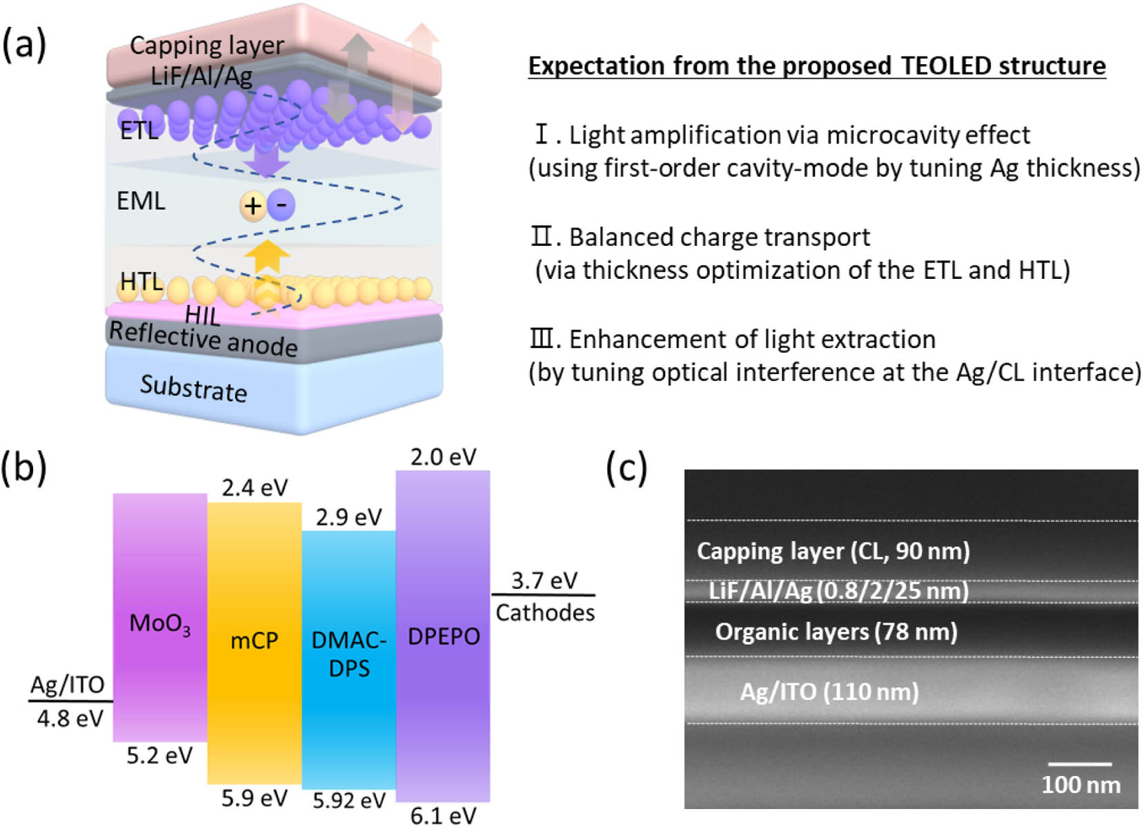
Figure 1.(a) Schematic of the TADF TEOLED structure. (b) Diagram of HOMO and LUMO energy level for materials. (c) FIB-SEM image of the optimized device structure.
To determine the structure for the microcavity effect, optical simulations were performed to optimize the thicknesses of the HTL and ETL prior to fabricating the TEOLED devices. Appendix A (Fig. 7) shows the simulation modeling diagrams and refractive indices of the organic materials. The radiance intensity gradually decreases with the increasing HTL and ETL thickness, with a periodic intensity profile depending on the cavity length as shown in Fig. 2(a). Conventionally, relatively thick (
![]()
Figure 2.(a) Simulated e-field distribution of the microcavity as a function of the HTL and ETL thickness. Each part indicated by the arrow is the thickness range of the HTL and ETL that satisfies the first-, second-, and third-order microcavity condition, respectively. (b) Simulated e-field intensity distribution of the microcavity as a function of the HTL and ETL thickness in the first-order condition (part 1: 15 nm HTL and 35 nm ETL; part 2: 25 nm HTL and 25 nm ETL; part 3: 35 nm HTL and 15 nm ETL). Schematic energy band diagrams of the (c) HOD and (d) EOD.
To begin with, the luminescence range in the first-order condition was divided into three parts as indicated in Fig. 2(b):part 1 based on thicker ETL, part 2 based on similar thickness of HTL and ETL, and part 3 based on thicker HTL. Then, the HODs and EODs based on the above conditions were fabricated as follows:
HTL/HIL and ETL blocked the electron injection from the cathode and the hole injection from the anode in the HOD and EOD, respectively. Thus, the hole and electron transport behavior in devices can be analyzed through the HOD and EOD with a single carrier (hole or electron) moving through the EML as shown in Figs. 2(c) and 2(d). Figures 2(e) and 2(f) show the J–V characteristics of the HODs and EODs with different thicknesses of HTLs and ETLs, respectively. Compared to HOD 2 (
B. Optical Properties of Cathode Configuration
The microcavity effect and luminous efficiency are directly affected by the top semitransparent electrode, so the optimum thickness of the Ag cathode is calculated as shown in Appendix A (Fig. 8). Based on this simulation result, the suitable thickness of the Ag layer was observed to be between 10 and 30 nm within the blue spectrum. Thus, LiF/Al/Ag cathodes were fabricated, and their optical properties were investigated by varying the thickness of Ag between 10 and 30 nm (Appendix B, Fig. 9). As shown in Appendix B [Figs. 9(a) and 9(b)], the transmittance decreases steadily with the increase in Ag thickness. Particularly, the thin LiF/Al/Ag cathode exhibits a lower transmittance (52.7%) at 478 nm than 10 nm pure Ag film, and the transmittance of the other electrodes based on the 15, 20, and 25 nm Ag layers decreased to 38.3%, 27.2%, and 19.1%, respectively.
When the Ag thickness is increased to 30 nm, the transmittance of the electrode is even less than 11%, which is obviously not conducive to the extraction of light. In contrast, the reflectance increases continuously as the Ag thickness decreases; for example, the reflectance of a 30 nm Ag layer electrode is close to 80%, while the reflectance of the electrode based on a 10 nm Ag layer (35.6%) is less than half of that, which is not sufficient to achieve an effective microcavity effect. Thus, it was decided to use 15, 20, and 25 nm Ag layers as the optimization objects of the cathodes. Thereafter, devices with reflective
![]()
Figure 3.Device performances of the TEOLEDs with different thicknesses of Ag layers: (a)
To acquire the TEOLED characteristics with low FWHM and high light extraction simultaneously, cathodes with multilayer structures were designed, in which a CL was deposited on the top metal electrode. By utilizing the capping effect at the interface between the CL and air under reasonable optical design, the light extraction and spectral distribution can be modulated effectively. Hence, an organic dielectric material (DPEPO) with a suitable refractive index (
![]()
Figure 4.Schematics of optical paths in TEOLEDs (a) without and (b) with CL, and (c) simulated e-field intensity of the TEOLEDs (based on 15, 20, 25 nm Ag layers) as functions of the CL thickness and wavelength.
For the device without CL, the up light wave (
Figures 4(a) and 4(b) represent the schematics of optical paths with and without CL in TEOLEDs. Figure 4(c) displays the e-field intensity distribution of devices based on 15, 20, and 25 nm Ag layers as a function of CL thickness. Indeed, compared to other devices, the device based on 25 nm Ag layer has a stronger microcavity effect and narrower emission spectrum due to the enhancement of the resonance effect in a specific wavelength range. According to the simulated results, each of the TEOLEDs based on Ag layers with different thicknesses shows an intensity peak value at CL of approximately 90 nm (at 478 nm). To verify the influence of the CL on the output light and microcavity effect inside the devices, the near e-field distributions of the devices with and without CL are shown in Fig. 5. For the devices without CL, the microcavity effect is achieved in these devices because of the reflectance of the top semitransparent electrode. However, emission light cannot escape from the device due to lower transmittance of the top semitransparent electrode, resulting in low light extraction [Figs. 5(a)–5(c)]. Conversely, for devices with 90 nm CL, due to the influence of
![]()
Figure 5.Near-field distribution of the TEOLEDs without CL based on (a) 15 nm, (b) 20 nm, and (c) 25 nm Ag layers, and with 90 nm CL based on (d) 15 nm, (e) 20 nm, and (f) 25 nm Ag layers.
C. Performances of Optimized TEOLEDs
To verify our simulation analysis, 50, 70, 90, 110, and 130 nm CL thicknesses were set as objects of discussion and devices based on 15, 20, and 25 nm Ag layers with different CL thicknesses were fabricated. The structure of the TEOLEDs is as follows: reflective anode/HIL (1 nm)/HTL (15 nm)/EML (28 nm)/ETL (35 nm)/LiF (0.8 nm)/Al (2 nm)/Ag (
![]()
Figure 6.Device performances of the TEOLEDs with different CL thicknesses on 25 nm Ag layer: (a)
4. CONCLUSIONS
In summary, we demonstrated a high-color-purity blue TADF TEOLED based on the first-order cavity mode using the cathode configuration of a 25 nm Ag layer and 90 nm organic CL with a calibrated EQE of 8.4% and CE of 13.8 cd/A. By utilizing the low current characteristics of the blue TADF OLEDs and tuning the charge balance mechanism of holes and electrons, the first-order cavity mode with short optical length was successfully applied to TEOLEDs. Notably, compared to the TADF OLEDs with no microcavity based on ITO electrodes (FWHM–84 nm, Appendix D, Fig. 12), the FWHM of the TEOLED based on the optimized cathodes was reduced to 41 nm, which can increase the practical application of TADF material in the light-emitting devices market. Furthermore, the LiF/Al/Ag/DPEPO cathode configuration shows excellent characteristics, which not only improve light extraction but also color purity simultaneously. Based on the above results, we believe that this study will promote the commercialization of TADF OLEDs.
APPENDIX A: SIMULATION DETAILS AND RESULTS
Figure?
![]()
Figure 7.Schematic of (a) simulation modeling and (b) refractive index information of organic materials.
![]()
Figure 8.Simulated e-field intensity of microcavity.
APPENDIX B: OPTICAL PROPERTIES OF LiF/Al/Ag CATHODES
Figures?
![]()
Figure 9.(a) Transmittance, (b) reflectance, and (c) absorption with respect to the sheet resistance of the LiF/Al/Ag electrode with different Ag thicknesses.
APPENDIX C: DEVICE PERFORMANCEs
Figures?
![]()
Figure 10.Device performances of the TEOLEDs with different CL thicknesses on 15 nm Ag layer: (a)
![]()
Figure 11.Device performances of the TEOLEDs with different CL thicknesses on 20 nm Ag layer: (a)
APPENDIX D: EL SPECTRA OF THE DEVICES
Figure?
![]()
Figure 12.EL spectra of TADF OLEDs with first-order microcavity and without microcavity at 10 V.
References
[1] H. Uoyama, K. Goushi, K. Shizu, H. Nomura, C. Adachi. Highly efficient organic light-emitting diodes from delayed fluorescence. Nature, 492, 234-238(2012).
[2] Q. Zhang, B. Li, S. Huang, H. Nomura, H. Tanaka, C. Adachi. Efficient blue organic light-emitting diodes employing thermally activated delayed fluorescence. Nat. Photonics, 8, 326-332(2014).
[3] K. Goushi, K. Yoshida, K. Sato, C. Adachi. Organic light-emitting diodes employing efficient reverse intersystem crossing for triplet-to-singlet state conversion. Nat. Photonics, 6, 253-258(2012).
[4] J. Zhao, C. Zheng, Y. Zhou, C. Li, J. Ye, X. Du, W. Li, Z. He, M. Zhang, H. Lin, S. Tao, X. Zhang. Novel small-molecule electron donor for solution-processed ternary exciplex with 24% external quantum efficiency in organic light-emitting diode. Mater. Horiz., 6, 1425-1432(2019).
[5] Z.-P. Chen, D.-Q. Wang, M. Zhang, K. Wang, Y.-Z. Shi, J.-X. Chen, W.-W. Tao, C.-J. Zheng, S.-L. Tao, X.-H. Zhang. Optimization on molecular restriction for highly efficient thermally activated delayed fluorescence emitters. Adv. Opt. Mater., 6, 1800935(2018).
[6] Q. Zhang, D. Tsang, H. Kuwabara, Y. Hatae, B. Li, T. Takahashi, S. Y. Lee, T. Yasuda, C. Adachi. Nearly 100% internal quantum efficiency in undoped electroluminescent devices employing pure organic emitters. Adv. Mater., 27, 2096-2100(2015).
[7] K. Guo, H. Wang, Z. Wang, C. Si, C. Peng, G. Chen, J. Zhang, G. Wang, B. Wei. Stable Green phosphorescence organic light-emitting diodes with low efficiency roll-off using a novel bipolar thermally activated delayed fluorescence material as host. Chem. Sci., 8, 1259-1268(2017).
[8] Y. J. Cho, K. S. Yook, J. Y. Lee. A universal host material for high external quantum efficiency close to 25% and long lifetime in green fluorescent and phosphorescent OLEDs. Adv. Mater., 26, 4050-4055(2014).
[9] S.-W. Li, C.-H. Yu, C.-L. Ko, T. Chatterjee, W.-Y. Hung, K.-T. Wong. Cyanopyrimidine−carbazole hybrid host materials for high efficiency and low-efficiency roll-off TADF OLEDs. ACS Appl. Mater. Interfaces, 10, 12930-12936(2018).
[10] C. Murawski, K. Leo, M. C. Gather. Efficiency roll-off in organic light-emitting diodes. Adv. Mater., 25, 6801-6827(2013).
[11] C.-K. Moon, K. Suzuki, K. Shizu, C. Adachi, H. Kaji, J.-J. Kim. Combined inter- and intramolecular charge-transfer processes for highly efficient fluorescent organic light-emitting diodes with reduced triplet exciton quenching. Adv. Mater., 29, 1606448(2017).
[12] D. Zhang, X. Song, M. Cai, H. Kaji, L. Duan. Versatile indolocarbazole-isomer derivatives as highly emissive emitters and ideal hosts for thermally activated delayed fluorescent OLEDs with alleviated efficiency roll-off. Adv. Mater., 30, 1705406(2018).
[13] D. H. Ahn, H. Lee, S. W. Kim, D. Karthik, J. Lee, H. Jeong, J. Y. Lee, J. H. Kwon. Highly twisted donor−acceptor boron emitter and high triplet host material for highly efficient blue thermally activated delayed fluorescent device. ACS Appl. Mater. Interfaces, 11, 14909-14916(2019).
[14] T.-L. Wu, M.-J. Huang, C.-C. Lin, P.-Y. Huang, T.-Y. Chou, R.-W. Chen-Cheng, H.-W. Lin, R.-S. Liu, C.-H. Cheng. Diboron compound-based organic light-emitting diodes with high efficiency and reduced efficiency roll-off. Nat. Photonics, 12, 235-240(2018).
[15] K.-W. Tsai, M.-K. Hung, Y.-H. Mao, S.-A. Chen. Solution-processed thermally activated delayed fluorescent OLED with high EQE as 31% using high triplet energy crosslinkable hole transport materials. Adv. Funct. Mater., 29, 1901025(2019).
[16] Y.-K. Wang, C.-C. Huang, H. Ye, C. Zhong, A. Khan, S.-Y. Yang, M.-K. Fung, Z.-Q. Jiang, C. Adachi, L.-S. Liao. Through space charge transfer for efficient sky-blue thermally activated delayed fluorescence (TADF) emitter with unconjugated connection. Adv. Opt. Mater., 8, 1901150(2020).
[17] K. Duan, D. Wang, M. Yang, Z. Liu, C. Wang, T. Tsuboi, C. Deng, Q. Zhang. Weakly conjugated phosphine oxide hosts for efficient blue thermally activated delayed fluorescence organic light-emitting diodes. ACS Appl. Mater. Interfaces, 12, 30591-30599(2020).
[18] R. Furue, K. Matsuo, Y. Ashikari, H. Ooka, N. Amanokura, T. Yasuda. Highly efficient red–orange delayed fluorescence emitters based on strong π-accepting dibenzophenazine and dibenzoquinoxaline cores: toward a rational pure-red OLED design. Adv. Opt. Mater., 6, 1701147(2018).
[19] M. K. Etherington, J. Gibson, H. F. Higginbotham, T. J. Penfold, A. P. Monkman. Revealing the spin–vibronic coupling mechanism of thermally activated delayed fluorescence. Nat. Commun., 7, 13680(2016).
[20] Y. Kondo, K. Yoshiura, S. Kitera, H. Nishi, S. Oda, H. Gotoh, Y. Sasada, M. Yanai, T. Hatakeyama. Narrowband deep-blue organic light-emitting diode featuring an organoboron-based emitter. Nat. Photonics, 13, 678-682(2019).
[21] J. Li, D. Ding, Y. Wei, J. Zhang, H. Xu. A “Si-locked” phosphine oxide host with suppressed structural relaxation for highly efficient deep-blue TADF diodes. Adv. Opt. Mater., 4, 522-528(2016).
[22] X. Li, Y.-Z. Shi, K. Wang, M. Zhang, C.-J. Zheng, D.-M. Sun, G.-L. Dai, X.-C. Fan, D.-Q. Wang, W. Liu, Y.-Q. Li, J. Yu, X.-M. Ou, C. Adachi, X.-H. Zhang. Thermally activated delayed fluorescence carbonyl derivatives for organic light-emitting diodes with extremely narrow full width at half-maximum. ACS Appl. Mater. Interfaces, 11, 13472-13480(2019).
[23] S. Oda, B. Kawakami, R. Kawasumi, R. Okita, T. Hatakeyama. Multiple resonance effect-induced sky-blue thermally activated delayed fluorescence with a narrow emission band. Org. Lett., 21, 9311-9314(2019).
[24] R. E. Slusher, C. Weisbuch. Optical microcavities in condensed matter systems. Solid State Commun., 92, 149-158(1994).
[25] D. Poitras, C.-C. Kuo, C. Py. Design of high-contrast OLEDs with microcavity effect. Opt. Express, 16, 8003-8015(2008).
[26] R. H. Jordan, A. Dodabalapur, R. E. Slusher. Efficiency enhancement of microcavity organic light emitting diodes. Appl. Phys. Lett., 69, 1997-1999(1996).
[27] H. Peng, J. Sun, X. Zhu, X. Yu, M. Wong, H.-S. Kwok. High-efficiency microcavity top-emitting organic light-emitting diodes using silver anode. Appl. Phys. Lett., 88, 073517(2006).
[28] M. J. Park, S. K. Kim, R. Pode, J. H. Kwon. Low absorption semi-transparent cathode for micro-cavity top-emitting organic light emitting diodes. Org. Electron., 52, 153-158(2018).
[29] Y.-F. Liu, J. Feng, Y.-G. Bi, J.-F. Song, Y. Jin, Y. Bai, Q.-D. Chen, H.-B. Sun. Omnidirectional emission from top-emitting organic light-emitting devices with microstructured cavity. Opt. Lett., 37, 124-126(2012).
[30] M. Wang, J. Lin, Y.-C. Hsiao, X. Liu, B. Hu. A nanoporous polymer film as a diffuser as well as a light extraction component for top emitting organic light emitting diodes with a strong microcavity structure. Nanoscale, 8, 8575-8582(2016).
[31] T. Schwab, S. Schubert, S. Hofmann, M. Fröbel, C. Fuchs, M. Thomschke, L. Müller-Meskamp, K. Leo, M. C. Gather. Highly efficient color stable inverted white top-emitting OLEDs with ultra-thin wetting layer top electrodes. Adv. Optical Mater., 1, 707-713(2013).
[32] G. H. Kim, R. Lampande, J. B. Im, J. M. Lee, J. Y. Lee, J. H. Kwon. Controlling the exciton lifetime of blue thermally activated delayed fluorescence emitters using a heteroatom-containing pyridoindole donor moiety. Mater. Horiz., 4, 619-624(2017).
[33] V. Bulović, V. B. Khalfin, G. Gu, P. E. Burrows, D. Z. Garbuzov, S. R. Forrest. Weak microcavity effects in organic light-emitting devices. Phys. Rev. B, 58, 3730-3740(1998).
[34] L. Frédéric, A. Desmarchelier, R. Plais, L. Lavnevich, G. Muller, C. Villafuerte, G. Clavier, E. Quesnel, B. Racine, S. Meunier-Della-Gatta, J.-P. Dognon, P. Thuéry, J. Crassous, L. Favereau, G. Pieters. Maximizing chiral perturbation on thermally activated delayed fluorescence emitters and elaboration of the first top-emission circularly polarized OLED. Adv. Funct. Mater., 30, 2004838(2020).
[35] M. J. Park, Y. H. Son, G. H. Kim, R. Lampande, H. W. Bae, R. Pode, Y. K. Lee, W. J. Song, J. H. Kwon. Device performances of third order micro-cavity green top-emitting organic light emitting diodes. Org. Electron., 26, 458-463(2015).
[36] W. H. Lee, P. J. Jesuraj, H. Hafeez, D. H. Kim, C. M. Lee, S. H. Won, S. T. Shin, S. Park, T.-S. Bae, S. M. Yu, M. Song, C.-S. Kim, S. Y. Ryu. Comparison of organic light emitting diode performance using the spectroradiometer and the integrating sphere measurements. AIP Adv., 10, 095011(2020).
[37] E. F. Schubert, N. E. J. Hunt, M. Micovic, R. J. Malik, D. L. Sivco, A. Y. Cho, G. J. Zydzik. Highly efficient light-emitting diodes with microcavities. Science, 265, 943-945(1994).
[38] B. S. Chen, L. Deng, J. Xie, L. Peng, L. Xie, Q. Fan, W. Huang. Recent developments in top-emitting organic light-emitting diodes. Adv. Mater., 22, 5227-5239(2010).
[39] B. Hu, H. Chen, C. Li, W. Huang, M. Ichikawa. High-refractive-index capping layer improves top-light-emitting device performance. Appl. Opt., 59, 4114-4121(2020).
[40] S. K. Kim, R. Lampande, J. H. Kwon. Electro-optically efficient and thermally stable multilayer semitransparent pristine Ag cathode structure for top-emission organic light-emitting diodes. ACS Photon., 6, 2957-2965(2019).
[41] Y. Fu, X. Hu, Q. Gong. Silicon photonic crystal all-optical logic gates. Phys. Lett. A, 377, 329-333(2013).
[42] G. Antonacci, G. Lepert, C. Paterson, P. Török. Elastic suppression in Brillouin imaging by destructive interference. Appl. Phys. Lett., 107, 061102(2015).


Set citation alerts for the article
Please enter your email address

© Copyright 2018-2021 | Chinese Laser Press. All Rights Reserved 沪ICP备15018463号-20