Ning Liu, Xiaohong Yan, Long Gao, Sergey Beloshapkin, Christophe Silien, Hong Wei, "Ultrathin oxide controlled photocurrent generation through a metal–insulator–semiconductor heterojunction," Photonics Res. 10, 1996 (2022)
Copy Citation Text
Recent advances in nanoscale lasers, amplifiers, and nonlinear optical converters have demonstrated the unprecedented potential of metal–insulator–semiconductor (MIS) structures as a versatile platform to realize integrated photonics at the nanoscale. While the electric field enhancement and confinement have been discussed intensively in MIS based plasmonic structures, little is known about the carrier redistribution across the heterojunction and photocurrent transport through the oxide. Herein, we investigate the photo-generated charge transport through a single CdSe microbelt--Ag heterojunction with oxide thickness varying from 3 nm to 5 nm. Combining photocurrent measurements with finite element simulations on electron (hole) redistribution across the heterojunction, we are able to explain the loss compensation observed in hybrid plasmonic waveguides at substantially reduced pump intensity based on MIS geometry compared to its photonic counterpart. We also demonstrate that the MIS configuration offers a low-dark-current photodetection scheme, which can be further exploited for photodetection applications.
1. INTRODUCTION
Charge transport through a metal–insulator–semiconductor (MIS) heterogeneous junction holds the key to the performance of many classes of electronic devices, for example, MIS field-effect transistors and MIS capacitors [1]. In recent years, the MIS configuration has attracted great attention in the research community due to its novel applications in optical devices, in particular, nanoscale plasmonic devices such as hybrid plasmonic waveguides, hybrid plasmonic lasers [2–4], amplifiers [5], and nonlinear light conversion devices [6,7], in which the optical modes are tightly confined into a deep subwavelength scale of the interfaces of MIS, promoting strong light–matter interaction at the interfaces and bridging the size gap from a few nanometers of electronic components to a few micrometers of optical components.
For MIS based capacitors, the thickness of the insulator is usually larger than 5 nm to prevent any leakage current. For the application of ideal Schottky diodes, the insulator thickness is considered less than 1 nm. In photodetector applications, the insulator thickness is kept below 2 nm to allow an efficient carrier transport. In hybrid plasmonic structures, the thickness of the insulator is usually from 3 nm to 6 nm, allowing a strong electric field enhancement and a much reduced ohmic loss in the devices [8]. The interesting phenomenon of loss compensation in hybrid plasmonic waveguides at very low pump intensities was reported [5]. This demonstration opens up possibilities to significantly reduce the pump energy required to achieve gain-assisted signal modulation in plasmonic circuits. However, the mechanism is yet to be clarified. While the electric field enhancement and confinement have been discussed intensively in MIS based plasmonic structures, little is known about charge transport across the MIS heterojunction upon radiation of light, the redistribution of photo-generated carriers at the interfaces, their impacts on the optical gain/absorption of semiconductor material, and the potential application of MIS heterojunctions as photodetectors, particularly for oxide thickness ranging from 3 nm to 5 nm. Answers to above questions will also shed light on optically and electrically driven plasmonic signal modulation, which plays a pivotal role in integrated plasmonic circuits.
In this paper, we investigate the photocurrent transport through single CdSe microbelt interfaces with thickness varying from 3 nm to 5 nm. Peak photocurrent from a few nanoamperes to a few microamperes at peak incident laser intensity of with single photon energy exceeding the bandgap energy of CdSe is detected at zero bias for thickness , which is demonstrated through finite element simulation to be sensitively dependent on the positions of the conduction band edge of the ultrathin oxide layer. We show that the requirement for the aligned Fermi level across the heterojunction leads to a charge redistribution across the heterojunction and high optical gain in the CdSe region at low pump intensity. As the oxide thickness increases to 5 nm, no photocurrent is obtained at zero bias upon exposure to light. Instead, we observe an abrupt photocurrent increase at a moderate bias voltage of to , which is attributed to the Coulomb blockade effect. The current gain compared to dark current can exceed at a bias voltage of with a photoresponsivity of 0.03 A/W, which is of great importance for photodetection applications where low dark currents are highly desirable [9,10].
Sign up for Photonics Research TOC. Get the latest issue of Photonics Research delivered right to you!Sign up now
2. SAMPLE FABRICATION AND DARK CURRENT–VOLTAGE CHARACTERIZATION
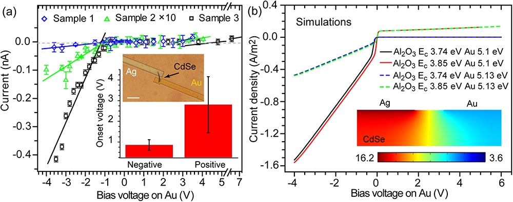
To fabricate the heterojunction, CdSe MBs grown by chemical vapor deposition are deposited on the glass coverslip first. The Au electrode is then deposited on one side of the chosen CdSe MB, followed by ultrathin layer growth via atomic layer deposition. Finally, the Ag electrode is formed on the other side of the CdSe MB (see Appendix A for details). One example of the final devices is given as an inset of Fig. 1(a). Before the photocurrent measurements are conducted, current–voltage (I-V) characteristics of the devices are obtained first without light. Figure 1(a) shows the typical dark I-V characteristics obtained on three devices with thickness . As the current through individual CdSe MB is extremely small (tens of picoamperes), a lock-in technique is used to obtain the current at ambient conditions and room temperature. In the measurements, the Ag electrode is kept at zero bias, while the voltage applied to the Au electrode varies (see Appendix A for details). It is clear from Fig. 1(a) that the absolute current is significantly larger for the negative bias voltage, behaving as a diode where the forward direction corresponds to the negative voltage. The absolute value of the current varies from one device to another, sensitively dependent on the thickness of CdSe MB, the contact area with the Au and Ag electrodes, and the lateral distance between the Au and Ag electrodes (see Appendix B). Out of 10 samples we measured with thickness , 70% of them showed measurable dark current. For devices with thickness , no dark current is detected within the bias range of to 9 V, meaning that the current is below the detection limit of our setup ().
Figure 1.Current–voltage characteristics across MB-Au heterojunction. (a) I-V characteristics of three samples of thickness . Data from sample 2 are multiplied by a factor of 10 for clarity. The onset voltages for six samples (three extra samples shown in Appendix C) are summarized into the histogram in the inset. The error bar indicates the standard deviation from all samples. The positive and negative onset voltages are the intersection voltages with the zero current axis obtained by linear fits to the data points in the corresponding voltage regions. The wide field optical image shows the heterojunction of sample 1 with the scale bar 5 μm. (b) COMSOL simulations on the I-V characteristics across (3 nm) -CdSe MB (500 nm)-Au heterojunction. In the simulations, the Ag work function and CdSe energy levels are kept the same while the conduction band of and Au work function are allowed to vary. The results demonstrate that the I-V can change significantly with even a small change in conduction band and Au work function. The inset shows the logarithm of electron density distribution, , at zero bias across the entire heterojunction with the conduction band of at 3.74 eV and Au work function of 5.13 eV. Here the unit of is .
The I-V characteristics of the devices observed experimentally can be reproduced using the finite element simulation package COMSOL Multiphysics 5.5 semiconductor module. The simulated I-V curves on a 500 nm thick CdSe MB with an thickness of 3 nm are plotted in Fig. 1(b). In the simulations, in addition to the drift-diffusion equations [1], tunneling of electrons through the layer and Au-CdSe Schottky barrier [11] is also included to properly reproduce the experimental I-V characteristics (see Appendices A and B for details). Here the work functions of Ag and Au are set at 4.6 eV [12] and 5.1 to 5.13 eV [13] while the conduction band and valence band of the CdSe are set to 4.5 eV and 6.23 eV [14], respectively. The band positions and bandgap of the ultrathin layer, on the other hand, have been reported with very different values in the literature, with the conduction band edge varying from 1.27 eV [15] to 3.8–4.7 eV [16,17], sensitively dependent on the thickness of the oxide, the growth temperature, and fabrication methods. Our simulations show that a small change in the conduction band position of the function of Au can lead to a large change in the tunneling current at the positive/negative voltage, as illustrated in Fig. 1(b).
One important result from the simulation is that even at zero bias, the electron density within the CdSe is much larger than the hole density within the CdSe due to the presence of Ag (see Appendix D for details). Since the conduction band edge of CdSe is very close to the work function of Ag, if a common Fermi level is assumed across the heterojunction at equilibrium, extra electrons are transferred from the Ag electrode to the CdSe region. This means that even at zero bias, the CdSe MB is negatively charged and the highest electron density within CdSe is located at the region closest to the Ag electrode. The electron density across the entire heterojunction at zero bias with electron affinity at 3.74 eV and Au work function at 5.13 eV is given in the inset of Fig. 1(b). This redistribution of free charges across the heterojunction has a significant impact on I-V characteristics.
3. PHOTOCURRENT CHARACTERISTICS FOR THICKNESS OF 3–4 nm
Upon exposure to light, the photocurrent through the MIS junction is observed for oxide thickness of 3 nm, as shown in Fig. 2. To measure the photocurrent, 532 nm pulsed laser light (Spark Antares laser, 80 MHz, pulse width 5–6 ps) is focused onto the sample by a 50× objective via an inverted Olympus microscope, as shown in Fig. 2(a). A wide field optical image of sample 1 with light focused on the CdSe heterojunction is displayed in Fig. 2(b). The generated photocurrent is also detected by a lock-in technique (see Appendix A for details). The calibrated peak currents as a function of bias voltage on the Au electrode for sample 1 and sample 4 are presented in Figs. 2(c) and 2(d), respectively. In both cases, we observed non-zero photocurrent at zero bias voltage. However, the polarity of photocurrent at zero bias varies from one sample to another. Among all samples, 25% exhibit positive current, 58% have negative current, and 17% have zero current at zero bias. We attribute the change in the polarity of zero bias photocurrent to the variation in the conduction band edge position of the ultrathin . As described in Figs. 2(e) and 2(f), the magnitude of photocurrent increases with the incident laser power even at zero bias. The simulated photocurrent curves, by the COMSOL semiconductor module in combination with the wave optics module, with the conduction band/Au work function at 3.74 eV/5.13 eV and 3.77 eV/5.1 eV are given in Figs. 2(g) and 2(h), respectively, and yield good agreement with experimental observations (see Appendix B for details). The photocurrent at zero bias is sensitively related to the local conduction band edge of , which can be related to the immobilized charges in the film [18,19] and the local work function of Au.
Figure 2.Photocurrent across (3–4 nm)-CdSe MB-Au heterojunction. (a) Diagram of experimental setup. (b) Wide field optical image showing the laser beam incident on the -CdSe MB heterojunction (sample 1). (c), (d) Peak photocurrent versus bias voltage on Au electrode of sample 1 and sample 4 at different incident laser powers. (e), (f) Zero bias photocurrent as a function of incident laser power for sample 1 and sample 4, respectively. The error bars indicate the fluctuation of reading from the lock-in amplifier. (g), (h) COMSOL simulation results of the photocurrent density versus bias voltage on Au electrode with conduction band at 3.74 eV (g) and 3.77 eV (h) and Au work function at 5.13 eV (g) and 5.1 eV (h) for incident laser power of . The simulated zero bias photocurrents as a function of incident laser power are given as insets.
4. IMPACT OF CARRIER REDISTRIBUTION ON OPTICAL ABSORPTION IN MB
The simulation model we developed to describe the photocurrents can also be used to evaluate the optical absorption properties of CdSe in this heterojunction. As the net optical absorption coefficient can be expressed as [20], where is the maximum absorption coefficient at photon energy of , and and are the electron occupancy factors in the valence band and conduction band at the given photon energy, respectively; and follow Fermi–Dirac distribution (see Appendix B for details) and can be obtained directly from the simulation model. The net optical absorption loss is therefore directly related to the difference in electron occupancy factors in the two bands. The band alignment across the heterojunction can directly influence the electron occupancy factors within the semiconductor. Figure 3(a) gives a diagram of the cross section used in the following simulations. The thicknesses of and CdSe are set as 3 nm and 200 nm, respectively. Figures 3(b) and 3(c) show energy diagrams at zero bias for the heterojunction and a model system, respectively. The model system assumes the metal work function positioned at the middle of the bandgap of CdSe as well as at that of the insulator. As discussed previously, the heterojunction allows the carriers to be redistributed to maintain the same effective Fermi level across the heterojunction. Figure 3(d) demonstrates the electron density distribution along the red line highlighted in Fig. 3(a) in the configuration [Fig. 3(b)] upon excitation of light at 532 nm as a function of position and incident power. Figure 3(f) gives the corresponding at the emission wavelength of 716 nm. As a comparison, we give the electron density distribution [Fig. 3(e)] and [Fig. 3(g)] of the model system [Fig. 3(c)]. The hole density, and distributions are given in Appendix E.
Figure 3.Impact of carrier redistribution on optical absorption loss in MB. (a) Diagram showing cross section and thicknesses of and CdSe used in this simulation. (b), (c) Energy diagrams of heterojunction and model system at zero bias, respectively. The affinity level (conduction band edge) of is set to 3.74 eV with a band gap of 2.6 eV. The work function of the metal in the model system is set to 5.366 eV, in the middle of CdSe bandgap. The bandgap of the oxide is set to 3 eV with the middle of the bandgap aligned with the metal work function. (d), (e) Electron density along the edge highlighted in red in (a) as a function of input power for (b) and the model system (c), respectively. The side plots give the electron density as a function of position at input power of 1 W. (f), (g) as a function of input power corresponding to (d) and (e) in the range from 0 nm to 80 nm, respectively. The side plots show the as a function of position at input power of 1 W.
It is clear from the plots that for the heterojunction, the electron density of CdSe is strongly enhanced in the region close to Ag due to the accumulation of electrons, which leads to a significantly decreased value. At the pump power of 1 W, at in Fig. 3(f), meaning that the absorption coefficient decreases to only 10% of the original value, while at in the model system without the transfer of carriers from the metal [Fig. 3(g)]. It is worth noting that the input power required to reach the onset of absorption loss reduction, for example, , occurs at input power of for , which is four orders of magnitude smaller compared to that needed for the model system (occurring at input power of 0.2 W). Our analysis reveals the mechanisms for the pump intensity reduction observed in gain-assisted loss compensation in hybrid plasmonic waveguides compared to their photonic counterparts [5]. These results suggest that in gain-assisted hybrid plasmonic signal propagation, the presence of metal not only allows light to be confined into a deep subwavelength volume, but the redistribution of carriers across the heterojunction also allows significant modulation to the output signal with only a fraction of pump energy as required to reach the same level of signal modulation in its photonic counterpart (more details can be found in Appendix F). This unique property can be very useful for all-optical signal modulation and computation [21,22].
5. ABRUPT PHOTOCURRENT INCREASE FOR THICKNESS LARGER THAN 4 nm
There is, however, a limitation on how thick the is allowed to be for the detection of photocurrent at zero bias. Once the thickness of increases to and above 4 nm, not only an energy gap is developed in the photocurrent I-V characteristics, but also a step-like feature is observed in the photocurrent as illustrated in Fig. 4(a). It is more intuitive to convert the peak current into the unit of electron number per 5 ps, as indicated by the right vertical axis of Fig. 4(a). The three curves are obtained from two different experimental setups (see Appendix A). The bottom curve is obtained with the same setup as used for Fig. 2 while the top two curves are obtained using a supercontinuum laser (repetition rate 40 MHz, pulse width), after passing through a bandpass filter. The curves for sample 2 and sample 6 are offset for clarity. The dashed lines indicate the zero current lines for each curve. From the curves shown in Fig. 4(a), we can see that only a few electrons transport through the heterojunction from each light pulse. This repeatable step-like negative current onset occurs between and 0.5 V, too small to be related to the avalanche effect [23]. We speculate that the sharp increase in photocurrent is caused by the Coulomb blockade effect commonly observed in single electron tunneling events through a double-barrier heterojunction [19,24–26]. In the current case, the tunneling most likely happens through a localized state within the film [16]. It is difficult to predict the Coulomb blockade energy, the energy required for the electron to overcome to tunnel into the localized state within the layer, from the current simulation model. However, we can estimate the value to be less than half of the energy gap observed in Fig. 4(a) and larger than the thermal energy of , therefore between 0.03 eV and 0.75 eV. Figure 4(b) shows the photocurrent as a function of bias voltage on Au for different incident laser powers for sample 6. As shown in the inset of Fig. 4(b), the generated photocurrent after the threshold voltage linearly depends on the incident laser power. The photocurrent also depends on the wavelength of excitation light and is substantially quenched upon exposure to light with a photon energy below the bandgap of CdSe, as shown in Appendix G.
Figure 4.Photocurrent across (4–5 nm)-CdSe MB-Au heterojunction. (a) Peak photocurrent as a function of bias voltage on Au for three devices measured with two different laser systems. The black and blue curves are offset for clarity. The dashed lines indicate the zero current lines for each curve. The arrows indicate the step-like onsets of photocurrents. Samples 5 and 6 were excited with a supercontinuum laser (repetition rate 40 MHz, pulse width ) after passing a bandpass filter (). The inset shows a wide field optical image of the laser spot focused on the MB heterojunction of sample 6, with scale bar of 5 μm. Sample 2 was excited with the Spark Antares laser at 532 nm (80 MHz, pulse width 5–6 ps). The peak input intensities associated with the three curves are , , and for samples 6, 5, and 2, respectively. (b) Sample 6 photocurrent as a function of bias voltage on Au for different incident laser powers. After the initial sharp increase, the current plateaus or follows a gradual linear increase. The inset shows the linear dependence of the plateaued current on the input power. The error bars indicate the range of current variation in the gradual linear increase regions.
In samples with of about 5 nm thickness, we have observed the onset voltage spanning from to (see Appendix H). These results suggest that once the thickness goes beyond 5 nm, carrier redistribution across the MIS junction may be ignored at zero bias. As mentioned previously, the dark current of devices with thickness of 5 nm is lower than the detection limit of our setup () in the bias range of to . Nevertheless, the peak photocurrent detected from these devices can exceed 70 μA at with a modest peak incident power of , giving a current gain larger than and a photoresponsivity of 0.03 A/W [27]. For bias voltage magnitude larger than 2 V, the avalanche effect caused by impact ionization may also contribute to the giant current gain [23,28]. With optimization of CdSe thickness and excitation method to maximize the absorption of light [27,29], the photoresponsivity value of this type of device can be further improved. The very low dark current is in sharp contrast with the high photocurrent detected upon exposure to light. The low operation voltage also makes MIS based photodetection very compatible with on-chip applications and can be easily incorporated in an integrated optoelectrical platform.
6. CONCLUSION
In conclusion, we have studied the photocurrent generation and transportation through the heterojunction with thickness varying from 3 nm to 5 nm. The direct observation of nonzero photocurrents at zero bias voltage in the oxide thickness range of suggests a charge redistribution across the heterojunction when CdSe is optically excited, and this charge redistribution leads to a substantially reduced optical absorption coefficient upon excitation of the hybrid plasmonic mode supported by the heterojunction, making gain-assisted plasmonic signal modulation possible at low pump intensity. As the thickness of the oxide increases to , the Coulomb blockade effect is observed in the photocurrents, corresponding to a sharp onset in the I-V characteristics. The extremely low dark current and large photocurrent detected upon exposure to light at relatively low voltage make this configuration a promising candidate in photodetection applications where low dark current and low bias voltages are of paramount importance.
Acknowledgment
Acknowledgment. We thank the Laboratory of Microfabrication in the Institute of Physics, Chinese Academy of Sciences, for experimental support. N. Liu acknowledges the support from the Irish Research Council “New Foundations” Programme and Science Foundation Ireland Career Development award. X. H. Yan, L. Gao, and H. Wei acknowledge the support from the National Natural Science Foundation of China, and the Strategic Priority Research Program of Chinese Academy of Sciences.
APPENDIX A: METHODS
Sample Fabrication
The CdSe MBs are grown by a chemical vapor deposition method. In short, an alumina boat containing CdSe powder is placed in the middle of a quartz tube furnace (single zone, Elite Thermal Systems). A Si substrate coated with a thin layer of Au () is then positioned at the downstream side of the tube. The furnace is first pumped down by a mechanical pump for 30 min. Ar gas is then introduced in the tube with a flow rate of 50 sccm (standard cubic centimeters per minute) while the pump is kept on. After the system is stabilized for 30 min, the furnace is heated up to 690°C and kept at this temperature for another 30 min for CdSe nanobelt growth. During growth, the Si sample is kept at a temperature of 500°C–600°C.
To fabricate the device for photocurrent measurements, an Au pad along with alignment marks is first defined on a glass coverslip by photolithography and deposited by thermal evaporation. CdSe MBs are then transferred onto the coverslip. An Au stripe (thickness 50 nm) connecting the Au pad and one side of the CdSe MB is defined by E-beam lithography and deposited by thermal evaporation. An ultrathin layer of is then deposited on the sample by atomic layer deposition. The thickness of the is measured by an ellipsometer or surface profilometer. Last, an Ag electrode (thickness 60 nm) is defined on the other side of the CdSe MB by E-beam lithography and deposited by thermal evaporation.
<i>I-V</i> Measurement without Light
The applied voltage is supplied by a square wave function generator, which is applied to the Au electrode of the sample. The current is then fed into the current port of a lock-in amplifier (Signal Recovery 7265) from the Ag electrode. The current is calibrated against a resistor of known value.
Photocurrent Detection
To measure the photocurrent, pulsed lasers (Spark Antares laser at 532 nm, 80 MHz, pulse width 5–6 ps or NKT SC-400 Supercontinuum laser, 40 MHz, pulse width 76–90 ps, 450 nm to 2.5 μm) are used. To extract the small photo-induced current, a lock-in technique is used. The reference frequency of the lock-in amplifier is taken from an optical chopper, which is used to modulate the on-and-off of the light focused on the sample at a low frequency (). The modulated light is directed into an inverted microscope (Olympus) and then focused onto the sample by a long working distance objective (Olympus, NA 0.55). A homemade LabVIEW program is used to control the voltage output/input from a National Instruments multifunction data acquisition (DAQ) device (NI USB-6212). The output voltage is applied to the Au electrode of the sample. The photocurrent is directly fed into the current port of a lock-in amplifier (Signal Recovery 7265) from the Ag electrode. The output voltage from the lock-in amplifier is then read back by the same LabVIEW program via the DAQ device.
COMSOL Simulation
The simulation on the I-V characteristic of the devices without and with exposure to light is carried out by the COMSOL Multiphysics simulation package 5.5 using the semiconductor module coupled with the wave optics module. Stationary study is used to calculate the I-V behavior without light and stationary-frequency study is used to calculate the photocurrent upon exposure to light (see Appendix B for more details).
APPENDIX B: COMSOL SIMULATIONS ON DARK CURRENT, PHOTOCURRENT, AND LOSS COMPENSATION
The semiconductor module in COMSOL 5.5 solves for the drift-diffusion equations of current density in the defined region: where is the electron density, the hole density, the electron charge, the conduction (valence) band energy level, the electron (hole) mobility, the Boltzmann constant, the lattice temperature, and and the thermal diffusion coefficients for electrons and holes, respectively. is the 1/2 order inverse Fermi–Dirac integral, and () is the effective density of states for electrons (holes) in the conduction (valence) band.
The solution also satisfies current continuity equations: where is the net electron (hole) recombination rate from all generation () and recombination mechanisms ().
The Wentzel–Kramers–Brillouin (WKB) tunneling model is used to allow tunneling current across the heterojunction to be calculated. Following Ref. [30], the electron normal thermionic current density across the heterojunction is multiplied by a factor of . The extra current factor is given by double integration along the electrical field line () and along the energy axis (): with and , where the second max function is taken within the potential barrier of , is the effective electron mass, and and are values of the conduction band energy in Ag and CdSe regions that are immediately outside of .
For direct bandgap semiconductors, the net generation rate due to stimulated emission can be evaluated as [20] where is the matrix element, is the reduced density of states, is the maximum absorption coefficient at photon energy of , and and are the electron occupancy factors for the conduction band and valence band, respectively, defined as where and are the quasi-Fermi levels of the conduction and valence bands, and and are energy levels of interest in the conduction band and valence band, respectively. To obtain net optical gain, the net generation rate due to stimulated emission needs to be larger than zero, which means , in other words, realizing population inversion. In a direct bandgap semiconductor, the energy levels of and are uniquely associated with photon energy , where . As discussed in detail in Ref. [20], and can be calculated following where and are conduction and valence band edge energy levels, respectively, is the bandgap energy of CdSe, and , , and are the effective electron mass, effective hole mass, and reduced mass of CdSe, respectively. From Eq. (B4), we can see that is closely related to the surrounding of CdSe through and . Appendix F gives two examples of .
The geometry we used to simulate the (3 nm)-CdSe (200 nm)-Au heterojunction is given in Fig. 5. A 2D model is used. The top-left boundary is set as the Ag electrode and the top-right boundary is set as the Au electrode. For the simulation of photocurrent, the input and output ports are highlighted by orange lines and red arrows. The input power is distributed on the input port assuming an area with a length indicated by the orange line (800 nm) and out of plane depth of 1 m. Figure 6 shows how the dark current across the heterojunction depends on the separation of Ag and Au electrodes and the thickness of CdSe MB.
Figure 5.Geometry of (3 nm)-CdSe (200 nm)-Au heterojunction defined in COSMOL.
APPENDIX C: DARK CURRENT-VOLTAGE CHARACTERISTICS OF MORE SAMPLES
Figure 7 shows the dark I-V characteristics of three more samples with thickness . Sample 5 was characterized with an old setup with larger noise.
APPENDIX D: HOLE DENSITY DISTRIBUTION AT ZERO BIAS WITHOUT EXPOSURE TO LIGHT
The hole density distribution at zero bias across the (3 nm)-CdSe (500 nm)-Au heterostructure is given in Fig. 8. The simulation parameters are the same as those used for the inset of Fig. 1(b).
APPENDIX E: HOLE DENSITY, fv, AND fc DISTRIBUTIONS RELATED TO FIG.?3
The distributions of hole density, , and at zero bias as a function of input power are shown in Fig. 9. Figures 9(a), 9(c), and 9(e) are simulated using the same parameters as those used for Fig. 3(d), and Figs. 9(b), 9(d), and 9(f) are simulated using the same parameters as those used for Fig. 3(e).
APPENDIX F: IMPACT OF CHARGE REDISTRIBUTION ACROSS Ag-Al2O3-CdSe ON GAIN-ASSISTED HYBRID PLASMONIC MODE PROPAGATION
As discussed in previous work [5], the propagation loss of the hybrid plasmonic mode supported by the heterostructure [inset of Fig. 10(a)] is significantly reduced at very low pump intensities. The threshold pump intensity, at which the loss compensation is observed, is 36 to 107 times smaller for a hybrid plasmonic waveguide than its photonic counterpart, in which the CdSe nanobelt is released on glass substrate [inset of Fig. 10(b)]. Figure 10 summarizes the results obtained from Ref. [5]. In these plots, the gain is defined as , where indicates the intensity of the output signal without pump light, the spontaneous emission intensity, and the intensity of the output signal with pump light.
As discussed in the main text, we can assume the absorption coefficient of CdSe as , where is the absorption coefficient without the pump light. As shown in Fig. 3 and Fig. 9, decreases with the pump power due to the increased and decreased values [in the case of Fig. 9(c), the band bending yields value close to one at low pump power]. Figure 11(a) displays the electric energy density distribution along (3 nm) -CdSe (200 nm) when the fundamental hybrid plasmonic mode at 716 nm is excited. The distribution shows that the electric energy density decreases rapidly away from the interface in the CdSe region, in a trend similar to Fig. 3(d). If we define an average occupancy difference as , where is the electric energy density along the dashed line highlighted in Fig. 11(a) and the position-dependent values are taken from Fig. 3(f), we can plot as a function of input power [Fig. 11(b)]. As a comparison, the values from the model system are also given in the same plot, which represents an approximation to the difference in electron occupancy factors for CdSe released on glass.
We can approximate the output intensity of light through a waveguide as where is the initial intensity of light at the start of the waveguide and the length of the waveguide. Without pump light, . With pump light, . So, and . Here is the distance on the waveguide that the pump light is on. If can be ignored when the intensity of the stimulated emission is much larger than that of the spontaneous emission, can be further expressed as
For a hybrid plasmonic waveguide, is usually much larger than that of the photonic waveguides. For the two waveguides shown in Fig. 10, the measured are and . From Eq. (F1) it is clear that the measured value is closely related to and for a given (2.5 μm in Ref. [5]). For the photonic waveguide, for , . For the hybrid plasmonic waveguide of , . This implies that loss compensation can be observed at much lower input power for a hybrid plasmonic waveguide, as shown in Fig. 11(b). The dashed lines guide the eyes to the threshold input power [], at which the dashed lines intercept with the top axis. These results are consistent with what were observed in Fig. 10.
Figure 6.Variation of dark current density across the (3 nm)-CdSe-Au heterojunction with the Ag and Au electrode separation (a) and thickness of the CdSe microbelt (b). The black curve in both panels is the same as the black curve in Fig. 1(b), with conduction band edge at 3.74 eV and Au work function at 5.1 eV. In current figure, all parameters are kept the same except for the one indicated in figure annotations. The thickness of the CdSe microbelt is 500 nm in (a), and the electrode separation is 400 nm in (b).
Figure 8.Hole density distribution () at zero bias across the (3 nm)-CdSe (500 nm)-Au heterostructure with conduction band of at 3.74 eV and Au work function of 5.13 eV.
Figure 10.Loss compensation measurements on the fundamental hybrid plasmonic mode supported on CdSe nanobelt- and photonic mode supported on CdSe nanobelt on glass. Plots are adapted from Ref. [5].
Figure 11.(a) Electric energy density distribution within (3 nm)-CdSe (200 nm thickness width) cross section when the fundamental hybrid plasmonic mode at 716 nm is excited. The side plot gives the electric energy density profile along the dashed line. The shadowed region indicates CdSe. (b) Electric energy density averaged for systems of with CdSe thickness of 200 nm, 100 nm, 50 nm, directly averaged over 10 nm in CdSe of 200 nm thickness closest to Ag, and for the model system. The dashed lines guide the eyes to the threshold input power, at which the dashed lines intercept with the top axis.
APPENDIX G: SPECTRAL DEPENDENCE OF THE PHOTOCURRENT
The photocurrent of sample 6 was measured at three different wavelengths, as shown in Fig. 12. The sample was excited with a supercontinuum laser (repetition rate 40 MHz, pulse width ) after passing through bandpass filters (, , and ). It is shown clearly that the photocurrent with 800 nm excitation is substantially smaller than those with 500 nm and 600 nm excitations.
Figure 12.Photocurrent measurements on sample 6 at three different wavelengths. (a) Typical photocurrent versus bias voltage at different incident laser wavelengths. The curve obtained from 800 nm excitation is multiplied by a factor of 20 for clarity. (b) Dependence of the plateaued current on the input power. The error bars indicate the range of current variation in the gradual linear increase regions.
APPENDIX H: PHOTOCURRENT I-V CHARACTERISTICS OF Ag-Al2O3 (5?nm)-CdSe MB-Au
Figure 13 shows the experimental results of peak photocurrent as a function of bias voltage for four samples with thickness . The samples were excited with a Spark Antares laser at 532 nm, with a repetition rate 80 MHz and pulse width 5–6 ps. The bias voltage for the negative photocurrent onset is in the range of to .
Figure 13.Photocurrent measurement on four samples of thickness around 5 nm. The peak input intensity is for samples 7 and 8, for sample 9, and for sample 10.
[1] S. M. Sze, K. K. Ng. Physics of Semiconductor Devices(2007).
[2] R. F. Oulton, V. J. Sorger, D. A. Genov, D. F. P. Pile, X. Zhang. A hybrid plasmonic waveguide for sub-wavelength confinement and long-range propagation. Nat. Photonics, 2, 496-500(2008).
[3] N. Liu, A. Gocalinska, J. Justice, F. Gity, I. Povey, B. McCarthy, M. Pemble, E. Pelucchi, H. Wei, C. Silien, H. Xu, B. Corbett. Lithographically defined, room temperature low threshold subwavelength red-emitting hybrid plasmonic lasers. Nano Lett., 16, 7822-7828(2016).
[4] R. F. Oulton, V. J. Sorger, T. Zentgraf, R.-M. Ma, C. Gladden, L. Dai, G. Bartal, X. Zhang. Plasmon lasers at deep subwavelength scale. Nature, 461, 629-632(2009).
[5] N. Liu, H. Wei, J. Li, Z. X. Wang, X. R. Tian, A. L. Pan, H. X. Xu. Plasmonic amplification with ultra-high optical gain at room temperature. Sci. Rep., 3, 1967(2013).
[6] Z. Li, B. Corbett, A. Gocalinska, E. Pelucchi, W. Chen, K. M. Ryan, P. Khan, C. Silien, H. Xu, N. Liu. Direct visualization of phase-matched efficient second harmonic and broadband sum frequency generation in hybrid plasmonic nanostructures. Light Sci. Appl., 9, 180(2020).
[7] J. Shi, Y. Li, M. Kang, X. He, N. J. Halas, P. Nordlander, S. Zhang, H. Xu. Efficient second harmonic generation in a hybrid plasmonic waveguide by mode interactions. Nano Lett., 19, 3838-3845(2019).
[8] H. Wei, D. Pan, S. Zhang, Z. Li, Q. Li, N. Liu, W. Wang, H. Xu. Plasmon waveguiding in nanowires. Chem. Rev., 118, 2882-2926(2018).
[9] R. Maiti, C. Patil, M. A. S. R. Saadi, T. Xie, J. G. Azadani, B. Uluutku, R. Amin, A. F. Briggs, M. Miscuglio, D. Van Thourhout, S. D. Solares, T. Low, R. Agarwal, S. R. Bank, V. J. Sorger. Strain-engineered high-responsivity MoTe2 photodetector for silicon photonic integrated circuits. Nat. Photonics, 14, 578-584(2020).
[10] A. H. Jones, S. D. March, S. R. Bank, J. C. Campbell. Low-noise high-temperature AlInAsSb/GaSb avalanche photodiodes for 2-μm applications. Nat. Photonics, 14, 559-563(2020).
[12] A. W. Dweydari, C. H. B. Mee. Work function measurements on (100) and (110) surfaces of silver. Phys. Status Solidi A, 27, 223-230(1975).
[13] D. R. Lide. CRC Handbook of Chemistry and Physics(2008).
[14] F. Buch, A. L. Fahrenbruch, R. H. Bube. Photovoltaic properties of five II-VI heterojunctions. J. Appl. Phys., 48, 1596-1602(1977).
[15] M. Kaltenbrunner, P. Stadler, R. Schwödiauer, A. W. Hassel, N. S. Sariciftci, S. Bauer. Anodized aluminum oxide thin films for room-temperature-processed, flexible, low-voltage organic non-volatile memory elements with excellent charge retention. Adv. Mater., 23, 4892-4896(2011).
[16] W. H. Rippard, A. C. Perrella, F. J. Albert, R. A. Buhrman. Ultrathin aluminum oxide tunnel barriers. Phys. Rev. Lett., 88, 046805(2002).
[17] F. Wang, N. A. Melosh. Plasmonic energy collection through hot carrier extraction. Nano Lett., 11, 5426-5430(2011).
[18] X. H. Qiu, G. V. Nazin, W. Ho. Vibrationally resolved fluorescence excited with submolecular precision. Science, 299, 542-546(2003).
[19] N. Liu. Atomic scale understanding of nanostructures in a double barrier tunneling junction: scanning tunneling microscopy of alkali doped buckminsterfullerenes on partially oxidized NiAl(110)(2005).
[20] O. Svelto. Principles of Lasers(2010).
[21] J. Feldmann, M. Stegmaier, N. Gruhler, C. Ríos, H. Bhaskaran, C. D. Wright, W. H. P. Pernice. Calculating with light using a chip-scale all-optical abacus. Nat. Commun., 8, 1256(2017).
[22] J. Feldmann, N. Youngblood, M. Karpov, H. Gehring, X. Li, M. Stappers, M. Le Gallo, X. Fu, A. Lukashchuk, A. S. Raja, J. Liu, C. D. Wright, A. Sebastian, T. J. Kippenberg, W. H. P. Pernice, H. Bhaskaran. Parallel convolutional processing using an integrated photonic tensor core. Nature, 589, 52-58(2021).
[23] O. Hayden, R. Agarwal, C. M. Lieber. Nanoscale avalanche photodiodes for highly sensitive and spatially resolved photon detection. Nat. Mater., 5, 352-356(2006).
[24] B. Su, V. J. Goldman, J. E. Cunningham. Observation of single-electron charging in double-barrier heterostructures. Science, 255, 313-315(1992).
[25] J. B. Barner, S. T. Ruggiero. Observation of the incremental charging of Ag particles by single electrons. Phys. Rev. Lett., 59, 807-810(1987).
[26] M. A. Reed, C. Zhou, C. J. Muller, T. P. Burgin, J. M. Tour. Conductance of a molecular junction. Science, 278, 252-254(1997).
[27] R. Gherabli, S. R. K. C. Indukuri, R. Zektzer, C. Frydendahl, U. Levy. MoSe2/WS2 heterojunction photodiode integrated with a silicon nitride waveguide for visible light detection with high responsivity(2021).
[28] Y.-J. Doh, K. N. Maher, L. Ouyang, C. L. Yu, H. Park, J. Park. Electrically driven light emission from individual CdSe nanowires. Nano Lett., 8, 4552-4556(2008).
[29] C. Frydendahl, M. Grajower, J. Bar-David, R. Zektzer, N. Mazurski, J. Shappir, U. Levy. Giant enhancement of silicon plasmonic shortwave infrared photodetection using nanoscale self-organized metallic films. Optica, 7, 371-379(2020).
[30] K. Yang, J. R. East, G. I. Haddad. Numerical modeling of abrupt heterojunctions using a thermionic-field emission boundary condition. Solid State Electron., 36, 321-330(1993).