• Journal of Inorganic Materials
  • Vol. 34, Issue 1, 37 (2019)
Lou-Wen ZHANG1, Shao-Li SHEN2, Lu-Ying LI2, Zhi ZHANG1, Ni-Shuang LIU1, Yi-Hua GAO1、2, [in Chinese]1, [in Chinese]2, [in Chinese]2, [in Chinese]1, [in Chinese]1, and [in Chinese]1、2
Author Affiliations
  • 11. School of Physics, Huazhong University of Science and Technology, Wuhan 430074, China
  • 22. Center for Nanoscale Characterization & Devices, Wuhan National Laboratory for Optoelectronics, Huazhong University of Science and Technology, Wuhan 430074, China;
  • show less
    DOI: 10.15541/jim20180176 Cite this Article
    Lou-Wen ZHANG, Shao-Li SHEN, Lu-Ying LI, Zhi ZHANG, Ni-Shuang LIU, Yi-Hua GAO, [in Chinese], [in Chinese], [in Chinese], [in Chinese], [in Chinese], [in Chinese]. Application and Development of Cesium Lead Halide Perovskite Based Planar Heterojunction LEDs[J]. Journal of Inorganic Materials, 2019, 34(1): 37 Copy Citation Text show less
    Optimization strategies for luminescence performance and stability of LED devices
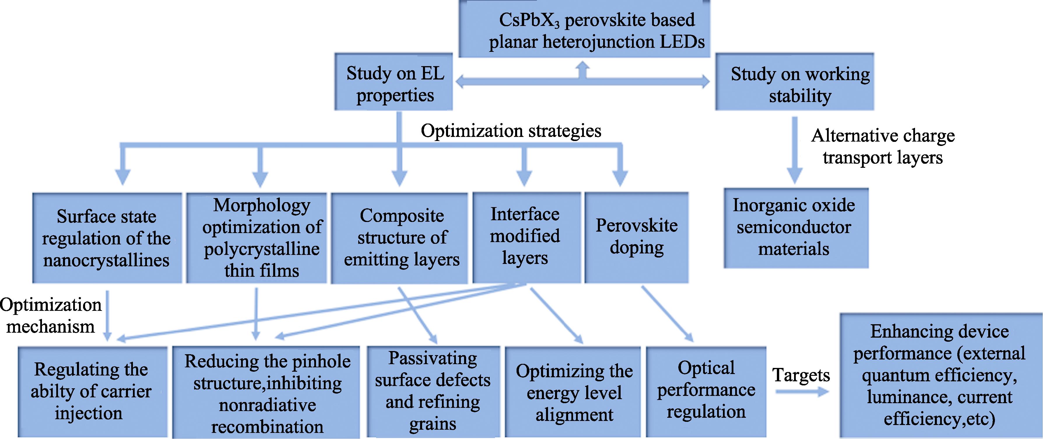
    . Optimization strategies for luminescence performance and stability of LED devices
    Schematic diagram of the device structures (a, b) and working mechanism (c) for perovskite based planar heterojunction LEDs
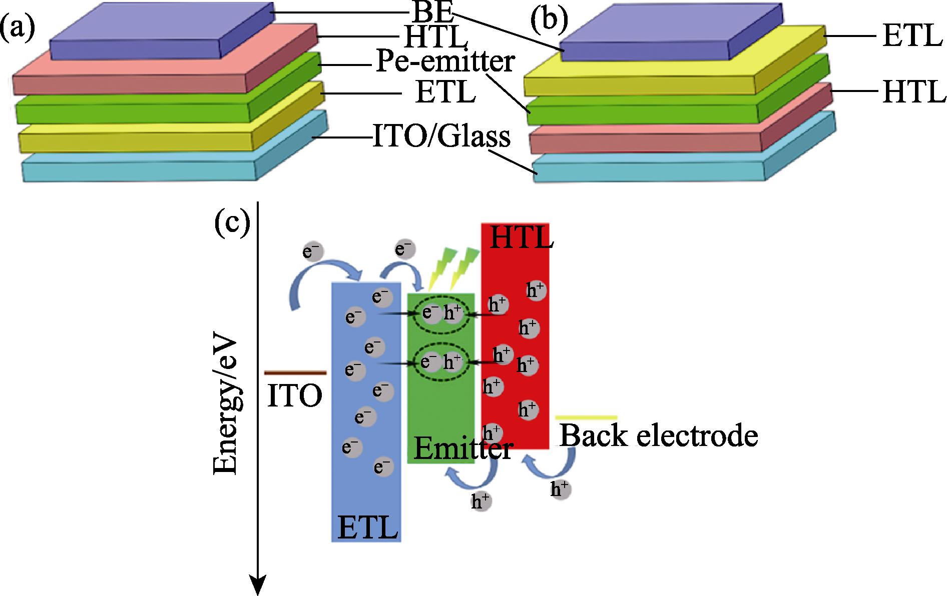
    . Schematic diagram of the device structures (a, b) and working mechanism (c) for perovskite based planar heterojunction LEDs
    (a) Schematic diagram of device structure; (b) Cross-sectional TEM image. Scale bar, 50 nm; (c) Flat-band energy level diagram; (d) The EL spectra (straight line) of devices for CsPb(Cl/Br)3, CsPbBr3 and CsPb(Br/I)3 under applied voltage of 5.5 V, and the photoluminescence (PL) spectra (dashed line) of QDs dispersed in hexane[58]
    . (a) Schematic diagram of device structure; (b) Cross-sectional TEM image. Scale bar, 50 nm; (c) Flat-band energy level diagram; (d) The EL spectra (straight line) of devices for CsPb(Cl/Br)3, CsPbBr3 and CsPb(Br/I)3 under applied voltage of 5.5 V, and the photoluminescence (PL) spectra (dashed line) of QDs dispersed in hexane[58]
    (a) Schematic illustration of device structure and a cross-sectional TEM image (scale bar: 50 nm); (b) Normalized EL spectra (solid lines) and PL spectra (dashed lines) of CsPbBr3 QLEDs with two purifying cycles. Inset in (b): The photograph of a working device at an applied voltage of 5 V; (c) EQE of these devices for QDs with different purifying cycles as a function of luminance[59]
    . (a) Schematic illustration of device structure and a cross-sectional TEM image (scale bar: 50 nm); (b) Normalized EL spectra (solid lines) and PL spectra (dashed lines) of CsPbBr3 QLEDs with two purifying cycles. Inset in (b): The photograph of a working device at an applied voltage of 5 V; (c) EQE of these devices for QDs with different purifying cycles as a function of luminance[59]
    (a) Structural representation of CsPbBr3 based LEDs; (b) Current efficiency-voltage (CE-V), and EQE-voltage (EQE-V) characteristic curves[68]; The surface morphology of CsPbBr3 film and surface luminous photo of LED (c) without treatment and (d) with chlorobenzene treatment[69]
    . (a) Structural representation of CsPbBr3 based LEDs; (b) Current efficiency-voltage (CE-V), and EQE-voltage (EQE-V) characteristic curves[68]; The surface morphology of CsPbBr3 film and surface luminous photo of LED (c) without treatment and (d) with chlorobenzene treatment[69]
    (a) EQE and CE as a function of voltage among devices fabricated with different ETL and HTL materials[77]; (b) EQE-V curves for the LEDs with different PEG:CsPbBr3 (CsBr:PbBr2 molar ratio of 1.4:1) weight ratios[78]; (c) TEM image of cross section of device and corresponding schematic diagram of device structure; (d) EQE for the devices with and without Ag rod[79]
    . (a) EQE and CE as a function of voltage among devices fabricated with different ETL and HTL materials[77]; (b) EQE-V curves for the LEDs with different PEG:CsPbBr3 (CsBr:PbBr2 molar ratio of 1.4:1) weight ratios[78]; (c) TEM image of cross section of device and corresponding schematic diagram of device structure; (d) EQE for the devices with and without Ag rod[79]
    (a) Overall energy band diagram of the LED structure; (b) EQE and CE vs current density of devices with or without PFI interface modifier[85]; (c) Schematic diagram of device structure; (d) CE and EQE of devices with and without PVP buffer layer, with and without CH3NH3Br (MABr) additive[51]
    . (a) Overall energy band diagram of the LED structure; (b) EQE and CE vs current density of devices with or without PFI interface modifier[85]; (c) Schematic diagram of device structure; (d) CE and EQE of devices with and without PVP buffer layer, with and without CH3NH3Br (MABr) additive[51]
    (a) Schematic illustration of device structure; (b) EQE of the devices as a function of luminance[90]; (c) Band alignment of each functional layer; (d) EQE of the devices as a function of driving voltage[91]
    . (a) Schematic illustration of device structure; (b) EQE of the devices as a function of luminance[90]; (c) Band alignment of each functional layer; (d) EQE of the devices as a function of driving voltage[91]
    (a) Simplified energy band alignment of the LED; (b) Luminous efficiency and EQE versus voltage of the LED[99]; (c) Schematic illustration of solution-processed perovskite LED; (d) EQE, CE, and power efficiency versus voltage of the LED[102]
    . (a) Simplified energy band alignment of the LED; (b) Luminous efficiency and EQE versus voltage of the LED[99]; (c) Schematic illustration of solution-processed perovskite LED; (d) EQE, CE, and power efficiency versus voltage of the LED[102]
    Lou-Wen ZHANG, Shao-Li SHEN, Lu-Ying LI, Zhi ZHANG, Ni-Shuang LIU, Yi-Hua GAO, [in Chinese], [in Chinese], [in Chinese], [in Chinese], [in Chinese], [in Chinese]. Application and Development of Cesium Lead Halide Perovskite Based Planar Heterojunction LEDs[J]. Journal of Inorganic Materials, 2019, 34(1): 37
    Download Citation