• Chinese Optics Letters
  • Vol. 17, Issue 2, 020011 (2019)
Jiandong Qiao1, Fuhong Mei1, and Yu Ye2、3、*
Author Affiliations
  • 1Key Laboratory of Interface Science and Engineering in Advanced Materials, Ministry of Education, Taiyuan University of Technology, Taiyuan 030024, China
  • 2State Key Laboratory for Artificial Microstructure & Mesoscopic Physics, School of Physics, Peking University, Beijing 100871, China
  • 3Collaborative Innovation Center of Quantum Matter, Beijing 100871, China
  • show less
    DOI: 10.3788/COL201917.020011 Cite this Article Set citation alerts
    Jiandong Qiao, Fuhong Mei, Yu Ye. Single-photon emitters in van der Waals materials[J]. Chinese Optics Letters, 2019, 17(2): 020011 Copy Citation Text show less
    Single-photon emitters in 2D materials. (a) Photoluminescence (PL) intensity map of narrow emission lines within a spectral width of 12 meV centered at 1.719 eV, over a 25 μm × 25 μm area. The dashed triangle indicates the position of the monolayer[18]. (b) PL spectrum of localized emitters. The left inset is a high-resolution spectrum of the highest intensity peak. The right inset is a zoom-in of the monolayer exciton emission. The emission of the localized emitters exhibits a red shift and much sharper spectral lines[18]. (c) Second-order correlation measurement of the PL from quantum emission under a 6.8 μW continuous wave (CW) laser excitation at 637 nm. The red line is a fit to the data with an extracted g2(0) of 0.14 ± 0.04[18]. (d) Scanning confocal map of a multilayer hBN sample showing bright luminescent spots, some of which correspond to emission from single defects[22]. (e) Room-temperature PL spectra of a defect center in hBN monolayer (blue trace) and multilayer (red trace)[22]. (f) Fluorescence saturation curve obtained from a single defect, showing a maximum emission rate of 4.26 MHz[22].
    Fig. 1. Single-photon emitters in 2D materials. (a) Photoluminescence (PL) intensity map of narrow emission lines within a spectral width of 12 meV centered at 1.719 eV, over a 25μm×25μm area. The dashed triangle indicates the position of the monolayer[18]. (b) PL spectrum of localized emitters. The left inset is a high-resolution spectrum of the highest intensity peak. The right inset is a zoom-in of the monolayer exciton emission. The emission of the localized emitters exhibits a red shift and much sharper spectral lines[18]. (c) Second-order correlation measurement of the PL from quantum emission under a 6.8μW continuous wave (CW) laser excitation at 637 nm. The red line is a fit to the data with an extracted g2(0) of 0.14±0.04[18]. (d) Scanning confocal map of a multilayer hBN sample showing bright luminescent spots, some of which correspond to emission from single defects[22]. (e) Room-temperature PL spectra of a defect center in hBN monolayer (blue trace) and multilayer (red trace)[22]. (f) Fluorescence saturation curve obtained from a single defect, showing a maximum emission rate of 4.26 MHz[22].
    Deterministic activation single-photon emitters in 2D materials. (a) Mechanism illustration of the generation of single-photon emitters in WSe2 by induced strain[65]. (b) Optical micrograph of bi-layer WSe2 after the transfer onto the nanopillars[65]. (c) A 2D spatial map of the PL integrated intensity within 700–860 nm[65]. (d) Photon quantum correlation characterization from a bi-layer emitter with a g(2)(0) of 0.03 ± 0.02[65]. (e) Schematic illustration of a ∼20 nm-thick hBN conformed on a nanostructured silica substrate[66]. (f) Three-dimensional atomic force microscope (AFM) image of a folded ∼20 nm-thick hBN on nanopillars[66]. (g) Room-temperature confocal (main) and optical (inset) images of an example nanopillars structure for spacings of 2 μm (left and center arrays) and 3 μm (far right); the pillar height is 155 nm, while the pillar diameter varies from 250 nm for the lower left-hand array to 500 nm for the top center array in increments of 50 nm[66]. (h) PL spectrum from an active pillar site. The relatively sharp ZPL and phonon replica suggest that the emission originates from a single defect[66]. (i) Statistic analysis of peak wavelength of the emitters, showing a broad distribution from 530 to 620 nm[66].
    Fig. 2. Deterministic activation single-photon emitters in 2D materials. (a) Mechanism illustration of the generation of single-photon emitters in WSe2 by induced strain[65]. (b) Optical micrograph of bi-layer WSe2 after the transfer onto the nanopillars[65]. (c) A 2D spatial map of the PL integrated intensity within 700–860 nm[65]. (d) Photon quantum correlation characterization from a bi-layer emitter with a g(2)(0) of 0.03±0.02[65]. (e) Schematic illustration of a 20nm-thick hBN conformed on a nanostructured silica substrate[66]. (f) Three-dimensional atomic force microscope (AFM) image of a folded 20nm-thick hBN on nanopillars[66]. (g) Room-temperature confocal (main) and optical (inset) images of an example nanopillars structure for spacings of 2μm (left and center arrays) and 3μm (far right); the pillar height is 155 nm, while the pillar diameter varies from 250 nm for the lower left-hand array to 500 nm for the top center array in increments of 50 nm[66]. (h) PL spectrum from an active pillar site. The relatively sharp ZPL and phonon replica suggest that the emission originates from a single defect[66]. (i) Statistic analysis of peak wavelength of the emitters, showing a broad distribution from 530 to 620 nm[66].
    Electrically driven single-photon emission in layered materials. (a) Optical microscope image of a typical single-photon emission LED[67]. (b) At 0.570 μA (1.97 V), highly localized emission dominates over the WS2 exciton emission[67]. (c) Intensity-correlation function g(2)(τ) for the same QD displaying the antibunched nature of the electroluminescence signal with a g(2)(0) of 0.31 ± 0.05[67]. (d) Schematic illustration of the vdW heterostructure used to form an electrically pumped quantum emission light-emitting device[68]. (e) Electroluminescence from the single defect as a function of energy and bias[69]. (f) Electroluminescence from the lateral LED as a function of polarization detection angle[69].
    Fig. 3. Electrically driven single-photon emission in layered materials. (a) Optical microscope image of a typical single-photon emission LED[67]. (b) At 0.570μA (1.97 V), highly localized emission dominates over the WS2 exciton emission[67]. (c) Intensity-correlation function g(2)(τ) for the same QD displaying the antibunched nature of the electroluminescence signal with a g(2)(0) of 0.31±0.05[67]. (d) Schematic illustration of the vdW heterostructure used to form an electrically pumped quantum emission light-emitting device[68]. (e) Electroluminescence from the single defect as a function of energy and bias[69]. (f) Electroluminescence from the lateral LED as a function of polarization detection angle[69].
    Detuning. (a) Extracted central energies of the single-photon doublet in single-layer WSe2 as functions of the magnetic field[18]. (b) Experimental scheme used to apply strain to hBN flakes sitting on a bendable polycarbonate (PC) beam clamped at one edge[77]. (c) The plot shows the scaled energy shift as a function of applied strain to the bendable substrate for three emitters with different tunabilities of −3.1 meV/% (green), +3.3 meV/% (yellow), and +6 meV/% (red). Inset shows a sketch of a quadratic energy shift ΔE for the single-photon emission induced by intrinsic strain[77]. (d) Pressure-dependent energy blueshift of a WSe2 defect emission line[78]. (e) Pressure-dependent energy redshift of a WSe2 defect emission line[78]. (f) Defect emission line as a function of pressure, showing a redshift at a rate of 1.31(7) meV/GPa (peak A) initially, as well as a subsequent blueshift at a rate of 0.72(4) meV/GPa (peak B), respectively[78]. (g) Device schematics of multilayer hBN sandwiched by top and bottom few-layer graphene[79]. (h) Scanning PL image of the device measured at 10 K. The squared bright spot shows a localized defect emission[79]. (i) Stark shifts in a single-photon emitter[75].
    Fig. 4. Detuning. (a) Extracted central energies of the single-photon doublet in single-layer WSe2 as functions of the magnetic field[18]. (b) Experimental scheme used to apply strain to hBN flakes sitting on a bendable polycarbonate (PC) beam clamped at one edge[77]. (c) The plot shows the scaled energy shift as a function of applied strain to the bendable substrate for three emitters with different tunabilities of 3.1meV/% (green), +3.3meV/% (yellow), and +6meV/% (red). Inset shows a sketch of a quadratic energy shift ΔE for the single-photon emission induced by intrinsic strain[77]. (d) Pressure-dependent energy blueshift of a WSe2 defect emission line[78]. (e) Pressure-dependent energy redshift of a WSe2 defect emission line[78]. (f) Defect emission line as a function of pressure, showing a redshift at a rate of 1.31(7) meV/GPa (peak A) initially, as well as a subsequent blueshift at a rate of 0.72(4) meV/GPa (peak B), respectively[78]. (g) Device schematics of multilayer hBN sandwiched by top and bottom few-layer graphene[79]. (h) Scanning PL image of the device measured at 10 K. The squared bright spot shows a localized defect emission[79]. (i) Stark shifts in a single-photon emitter[75].
    Integration of 2D single-photon emitters with photonic circuits. (a) Schematic illustration of the movement of a gold sphere to the hBN flake[81]. (b) Two Au particles are in contact with the hBN flake. Scale bar: 250 nm[81]. (c) A comparison of fluorescence saturation curves among between the pristine, single particle, and double particle arrangements[81]. (d) Schematic of single-layer WSe2 coupled to a plasmonic Au nanocube cavity array. The WSe2 is separated from the plasmonic Au cubes and the planar Au layer by a 2 nm Al2O3 spacer layer on each side to prevent optical quenching and short-circuiting of the nanoplasmonic gap mode[82]. (e) Spontaneous emission lifetime measurements recorded at 40 μW excitation power[82]. (f) Integrated PL intensity as a function of excitation power under 78 MHz pulsed excitation, comparing quantum emitters from chemical vapor transport (CVT)-grown WSe2 before (black circles) and after coupling (green circles) with quantum emitters created in flux-grown WSe2 before and after coupling[82]. (g) PL spectrum of a 1D cavity fabricated by focused ion-beam milling, showing a high-Q (∼2100) mode in the visible spectral range. The inset is a scanning electron microscope (SEM) image of the cavity, and the scale bar corresponds to 1 μm[83]. (h) PL map positions of quantum emitters are indicated by yellow circles[83]. (i) PL spectra from two regions of the same cavity showing an optical mode only (blue) and the combination of an optical mode and an emitter (red)[83].
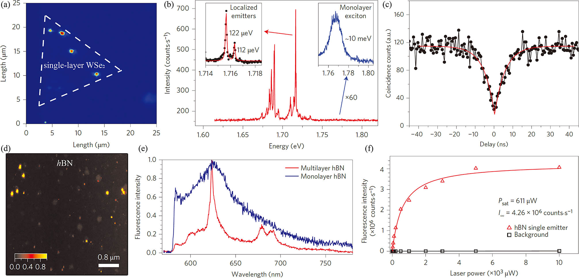
    Fig. 5. Integration of 2D single-photon emitters with photonic circuits. (a) Schematic illustration of the movement of a gold sphere to the hBN flake[81]. (b) Two Au particles are in contact with the hBN flake. Scale bar: 250 nm[81]. (c) A comparison of fluorescence saturation curves among between the pristine, single particle, and double particle arrangements[81]. (d) Schematic of single-layer WSe2 coupled to a plasmonic Au nanocube cavity array. The WSe2 is separated from the plasmonic Au cubes and the planar Au layer by a 2 nm Al2O3 spacer layer on each side to prevent optical quenching and short-circuiting of the nanoplasmonic gap mode[82]. (e) Spontaneous emission lifetime measurements recorded at 40μW excitation power[82]. (f) Integrated PL intensity as a function of excitation power under 78 MHz pulsed excitation, comparing quantum emitters from chemical vapor transport (CVT)-grown WSe2 before (black circles) and after coupling (green circles) with quantum emitters created in flux-grown WSe2 before and after coupling[82]. (g) PL spectrum of a 1D cavity fabricated by focused ion-beam milling, showing a high-Q (2100) mode in the visible spectral range. The inset is a scanning electron microscope (SEM) image of the cavity, and the scale bar corresponds to 1μm[83]. (h) PL map positions of quantum emitters are indicated by yellow circles[83]. (i) PL spectra from two regions of the same cavity showing an optical mode only (blue) and the combination of an optical mode and an emitter (red)[83].
    Jiandong Qiao, Fuhong Mei, Yu Ye. Single-photon emitters in van der Waals materials[J]. Chinese Optics Letters, 2019, 17(2): 020011
    Download Citation