Abstract
Solid-state sources of single-photon emitters are highly desired for scalable quantum photonic applications, such as quantum communication, optical quantum information processing, and metrology. In the past year, great strides have been made in the characterization of single defects in wide-bandgap materials, such as silicon carbide and diamond, as well as single molecules, quantum dots, and carbon nanotubes. More recently, single-photon emitters in layered van der Waals materials attracted tremendous attention, because the two-dimensional (2D) lattice allows for high photon extraction efficiency and easy integration into photonic circuits. In this review, we discuss recent advances in mastering single-photon emitters in 2D materials, electrical generation pathways, detuning, and resonator coupling towards use as quantum light sources. Finally, we discuss the remaining challenges and the outlooks for layered material-based quantum photonic sources.Emerging quantum technologies for cryptography, communication, computing, and metrology exploit non-classical states for enhanced information processing and nanoscale sensing[1,2]. Though different platform systems are currently being explored[3], light-based quantum technologies using single-photon emitters as the basic building block are among the frontrunners. A long-standing hurdle, however, has been the realization of robust, device-compatible single-photon emitters that can be activated and controlled on demand[4]. In the past, several different material systems have been used to realize deterministic single-photon sources in the solid state, including quantum dots (QDs), single molecules, carbon nanotubes, and point defects in wide-bandgap materials, such as diamond and silicon carbide[3,5–15]. However, these solid-state emitters are usually embedded in bulk materials with a high refractive index, where internal reflection may limit their integration capability and photon extraction efficiency[3]. Using carbon nanotube-based single-photon emitters in scalable quantum photonic applications requires precise placement and orientation using complex fabrication techniques[16,17]. Recently, the discovered single-photon emitters in crystalline two-dimensional (2D) materials[18–22], with their ultimate atomic thickness, have shown promise for precise placement, high extraction efficiency, and easy integration into photonic circuits[23–26]. Up to date, mechanical exfoliation of single crystals is still the most common way for producing 2D materials. Stride steps have been made recently in wafer-scale synthesis of 2D crystals, such as [27] and hexagonal boron nitride ()[28], opening a new route for large-scale quantum photonic applications. In addition, due to their flexibility, transfer 2D materials can be integrated with any other material that may alleviate the stringent requirement of epitaxial growth in traditional semiconductor materials. The van der Waals (vdW) materials containing single-photon emitters can potentially be compatible with other photonic components to fabricate vdW materials-based quantum photonic devices.
The discovered 2D systems hosting single-photon emitters include transition-metal dichalcogenides (TMDCs) (, , and ) and [18–22,29]. In particular, a defect hosted by 2D is a promising candidate for next-generation single-photon sources, due to its chemical and thermal robustness and high brightness at room temperature[22]. Here, we will first briefly review the available and most-studied single-photon emitters in layered materials and their photophysical properties. We will then discuss important steps towards deterministic generation of scalable 2D single-photon sources, electrically pumped quantum sources, detuning, and integration of emitters with optical resonators. We conclude with a discussion of challenges and highlight new research directions.
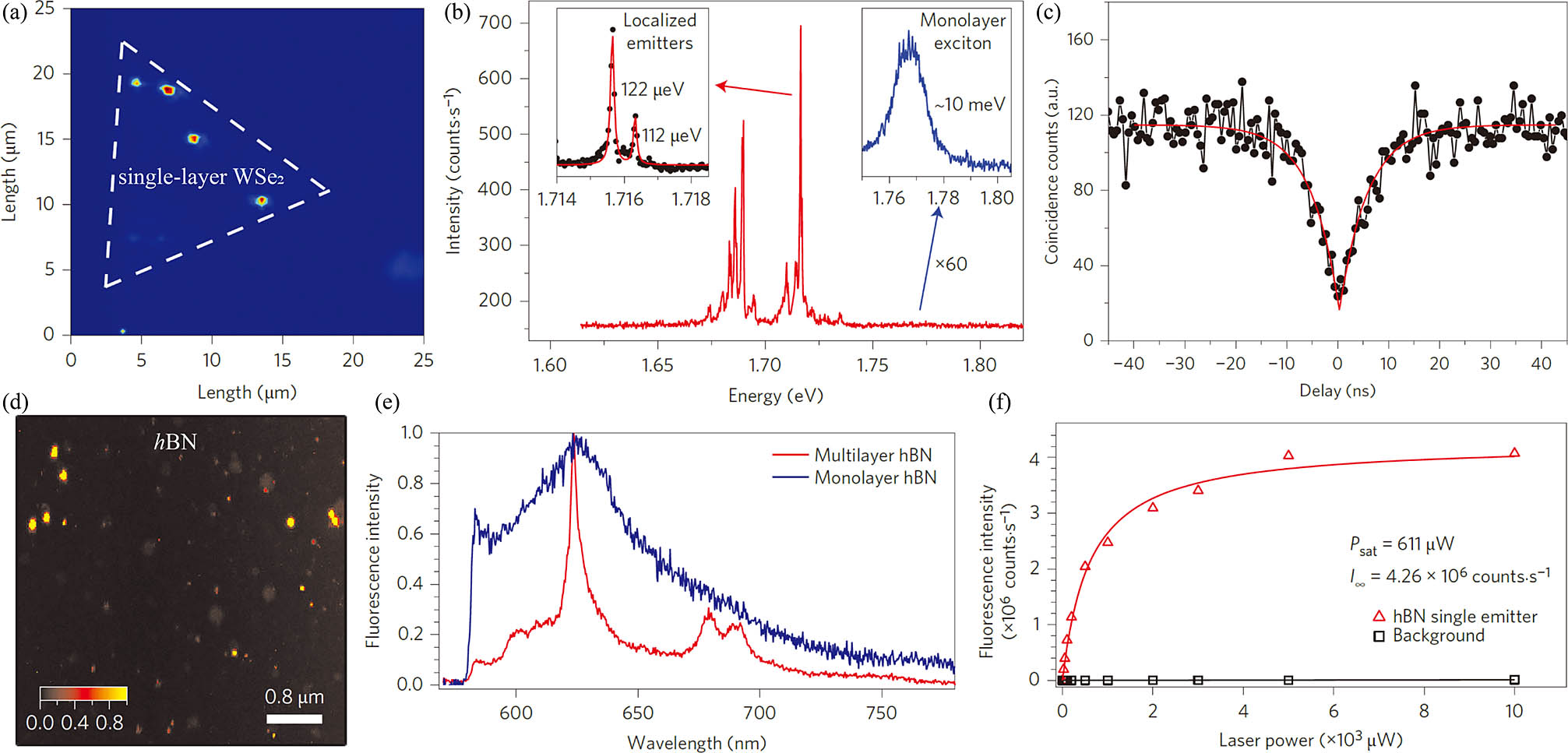
Single-photon emitters in 2D materials. Recently, a number of 2D materials have been shown to host single-photon emitters. The first observation of a single-photon emitter in layered materials was reported by four independent studies in the presence of isolated defects in single-layer [Fig. 1(a)][18–21]. TMDC monolayers have moved to the forefront of solid-state research due to their unique band structure featuring a large bandgap with non-equivalent valleys and non-zero Berry curvature[30]. The single-photon emitters in single-layer induced by the quantum defects are ascribed to localized, weakly bound excitons. Similarly to QDs, the TMDCs only exhibit quantum emission at cryogenic temperatures. In contrast to the free exciton emission with a broad linewidth of , the emission linewidths of these quantum defects are of only [Fig. 1(b)]. The emission is red shifted by from the free exciton transition. The brightness varies from sample to sample[31]. It was, however, also found that the quantum emitters in predominantly appear near 2D-layer interfaces, edges, and wrinkles and can be deliberately induced by tearing the monolayer lattice[32]. Photon antibunching from correlation measurements shows that they are single-photon emitters [Fig. 1(c)] with a value of 0.1–0.3. Most of the quantum emissions exhibit strong Zeeman shifts with an applied magnetic field with a factor of , which is much larger than those of the excitons in self-assembled InGaAs QDs[33] and free excitons in single-layer [34–36]. Unfortunately, the single-photon emission of single-layer and other TMDCs can only be obtained at cryogenic temperatures[18–21,29], which limits their practical applications in photonic quantum information.
Sign up for Chinese Optics Letters TOC. Get the latest issue of Chinese Optics Letters delivered right to you!Sign up now
![Single-photon emitters in 2D materials. (a) Photoluminescence (PL) intensity map of narrow emission lines within a spectral width of 12 meV centered at 1.719 eV, over a 25 μm × 25 μm area. The dashed triangle indicates the position of the monolayer[18]. (b) PL spectrum of localized emitters. The left inset is a high-resolution spectrum of the highest intensity peak. The right inset is a zoom-in of the monolayer exciton emission. The emission of the localized emitters exhibits a red shift and much sharper spectral lines[18]. (c) Second-order correlation measurement of the PL from quantum emission under a 6.8 μW continuous wave (CW) laser excitation at 637 nm. The red line is a fit to the data with an extracted g2(0) of 0.14 ± 0.04[18]. (d) Scanning confocal map of a multilayer hBN sample showing bright luminescent spots, some of which correspond to emission from single defects[22]. (e) Room-temperature PL spectra of a defect center in hBN monolayer (blue trace) and multilayer (red trace)[22]. (f) Fluorescence saturation curve obtained from a single defect, showing a maximum emission rate of 4.26 MHz[22].](/Images/icon/loading.gif)
Figure 1.Single-photon emitters in 2D materials. (a) Photoluminescence (PL) intensity map of narrow emission lines within a spectral width of 12 meV centered at 1.719 eV, over a area. The dashed triangle indicates the position of the monolayer[18]. (b) PL spectrum of localized emitters. The left inset is a high-resolution spectrum of the highest intensity peak. The right inset is a zoom-in of the monolayer exciton emission. The emission of the localized emitters exhibits a red shift and much sharper spectral lines[18]. (c) Second-order correlation measurement of the PL from quantum emission under a continuous wave (CW) laser excitation at 637 nm. The red line is a fit to the data with an extracted of [18]. (d) Scanning confocal map of a multilayer sample showing bright luminescent spots, some of which correspond to emission from single defects[22]. (e) Room-temperature PL spectra of a defect center in monolayer (blue trace) and multilayer (red trace)[22]. (f) Fluorescence saturation curve obtained from a single defect, showing a maximum emission rate of 4.26 MHz[22].
Defects in are the most recent addition into the single-photon emitter library and among the brightest single-photon emitters reported so far [Fig. 1(d)][37]. Single-photon emitters hosted by 2D are a promising candidate for next-generation single-photon sources due to their chemical and thermal robustness[38] and high brightness at room temperature. The single-photon emitters in were believed to be associated with defects within the large bandgap ()[39], whereas they give rise to deep states that allow single-photon emitters to operate at room temperature[40]. The single-photon emitters were obtained in both the liquid-intercalated few-layer and chemical vapor deposited single-layer [Fig. 1(e)]. Megahertz count rates at the detector have been recorded with a very low excitation power of several hundred microwatts [Fig. 1(f)]. The majority of photons are emitted into the zero-phonon line (ZPL) with clearly observed photon side bands[22]. However, the ZPL wavelength varies from sample to sample in a large wavelength range[41]. The nature of the single-photon emitter in is yet to be clarified, although some theoretical predictions exist[22,42]. Rigorous modeling along with atomic resolution characterizations needs to be carried out to reveal the electronic and crystallographic structure of the emitters.
Given that the single-photon emitter is embedded in a 2D material, it inherits the 2D material’s intrinsic physical properties, making it an exotic quantum building block for quantum techniques. These recently emerged 2D materials have been demonstrated to have remarkable mechanical, electronic, and optical properties that are absent in their bulk form[43–46]. These properties are widely tunable by doping, strain, external fields, and environmental effects, owing to the material’s atomic thickness[47]. Compared with other TMDCs, is the most-studied material[48] because it is the only material that exists in nature (molybdenite), and large-scale synthesis of single-layer is now mature in the industrial level[27]. The flexible 2D membranes can also be easily integrated into other systems or devices[49–51] or stacked layer-by-layer to form heterostructures with desired functionalities without the lattice matching constraint[52–54]. In addition, TMDC monolayers without inversion symmetry exhibit strong valley degrees of freedom[55–57]. The systematic study of the photophysical properties of single-photon emitters in layered materials needs to be carried out.
Deterministic activation of single-photon emitters. Although high-brightness single-photon emitters have been discovered in at room temperature, the samples were prepared in solution, suffering from problematic agglomeration[22]. To take advantage of 2D materials of easy integration with cavities and photonic waveguides, activation of the single-photon emitters in exfoliated or as-grown is necessary. The emitters can be activated in 2D by chemical etching[58], ion implantation[58], electron-beam (e-beam) irradiation[59], focused laser irradiation[60], argon plasma etching[61], high-energy electron irradiation[62], neutron irradiation[63], etc. Different methods produce different single-photon emitter generation rates. It was, however, also found that the quantum emitters in predominantly/randomly appear near 2D-layer interfaces, edges, and wrinkles[60]. In addition, in the whole process of quantum communication, except simple quantum key distribution (QKD) without quantum repeaters, the quantum light source needs to meet the requirement of emitting the indistinguishable single photons. The indistinguishable single photons require long coherence time with lifetime-limited linewidths. However, the room-temperature operation could be incompatible with this requirement due to their short coherence time. Moreover, the room-temperature single-photon emitter in suffers from increased multiphoton emission events with in the range of 0.1–0.3, although, many have very high emission rates of the order counts per second. This is also a barrier that single-photon emitters cannot be applied in actual quantum communication. Recently, a room-temperature ultra-narrow zero-phonon linewidth down to in quantum emitters could be achieved by proper surface passivation[64]. Still, deterministic placement of the single-photon emitters and control over a large scale are necessary for on-chip applications.
While nanobubbles as well as lithographic nanopillars in contact with the 2D materials act as spatially controlled stressors[32,65,66], the induced strain can then create excitons at defined locations [Fig. 2(a)]. This ability to create zero-dimensional (0D) excitons anywhere within 2D materials is promising for the development of scalable quantum technologies. Owing to the vdW force, a 2D flake conforms to the contours of a lithographically patterned nanopillar lattice [Fig. 2(b)]. The first demonstration of a quantum emitter array has been pursued by positioning the exfoliated flakes on top of lithographically predefined dielectric nanopillars[65]. In a bi-layer , a significant increase () in the peak photoluminescence intensity at the nanopillar sites was observed [Fig. 2(c)], evidencing the transition to a direct electronic gap and the exciton funnel effect due to local strain. Bright narrow-linewidth () emissions are observed at the strain-induced sites. The quantum nature of the single-photon emitters was evidenced by the second-order correlations from each individual peak, exhibiting highly pure single-photon emission with a of and a decay time of . The straightforward fabrication procedure is scalable. By tuning the aspect ratio of the nanopillars, it was able to obtain near unity success in generating an emitter at each nanopillar and a positioning accuracy of 120 nm. Owing to the smaller bandgap of , these strain-induced single-photon emitters could only operate at sufficiently low temperatures.
Figure 2.Deterministic activation single-photon emitters in 2D materials. (a) Mechanism illustration of the generation of single-photon emitters in by induced strain[65]. (b) Optical micrograph of bi-layer after the transfer onto the nanopillars[65]. (c) A 2D spatial map of the PL integrated intensity within 700–860 nm[65]. (d) Photon quantum correlation characterization from a bi-layer emitter with a of [65]. (e) Schematic illustration of a -thick conformed on a nanostructured silica substrate[66]. (f) Three-dimensional atomic force microscope (AFM) image of a folded -thick on nanopillars[66]. (g) Room-temperature confocal (main) and optical (inset) images of an example nanopillars structure for spacings of (left and center arrays) and (far right); the pillar height is 155 nm, while the pillar diameter varies from 250 nm for the lower left-hand array to 500 nm for the top center array in increments of 50 nm[66]. (h) PL spectrum from an active pillar site. The relatively sharp ZPL and phonon replica suggest that the emission originates from a single defect[66]. (i) Statistic analysis of peak wavelength of the emitters, showing a broad distribution from 530 to 620 nm[66].
This nanopillar process is applicable to other 2D materials, such as , to generate single-photon emitters at room temperature. The nanoscale strain engineering of the few-atomic-layer films ( thick) via patterned nanopillar substrates was used to activate the defects [Fig. 2(e)]. Due to vdW forces, the film conforms to the surface topography of the nanopillars, resulting in significant local strain near the edges [Fig. 2(f)]. The light emission selectively originated from the nanopillar sites, showing a one-to-one correspondence with the underlying structure, independent of the spacing between pillars [Fig. 2(g)]. Due to large-scale chemical vapor deposition (CVD) of thin films, this process can be scalable. The spectrum from an example site shows a well-defined ZPL accompanied by multiple phonon replicas separated by about 165 meV [Fig. 2(h)]. Photon antibunching from correlation measurements shows a value of , indicating single-photon emission. The physics (local electrostatic potentials) at play is proven to be very different from the localized exciton-based single-photon emitters realized at cryogenic temperatures in flakes (strain) on patterned substrates, opening interesting opportunities for manipulating defect emission in via local gatings, surface chemistry, etc. The histogram of 80 single-photon emitters shows that emitters span a broad wavelength region from 530 to 620 nm [Fig. 2(i)], which is detrimental for quantum technologies.
This nanopillar process is expensive, as it requires e-beam lithography and a subsequent reactive ion-etching step. In addition, the vertical one-dimensional (1D) structure makes the hybrid single-photon emitter system bulky, making it hard to couple with cavity or waveguide modes for future cavity quantum electrodynamics experiments or integrated quantum photonic applications.
Electrically driven single-photon emission in layered materials. All-electrical single-photon emission is a key priority for integrated quantum technologies. In a scalable circuit, fully integrated devices require just a drive current to get the single-photon emission instead of using a laser that focuses on different segments of an integrated circuit[67–69]. Despite a plethora of single-photon sources reported to date, the all-electrical operation desired for system integration is only reported in the embedded systems[70,71]. Using recently developed techniques for mechanically assembling a vdW heterostructure layer-by-layer, researchers use layered materials to create all-electrical quantum light emitting diodes (LEDs) with single-photon emission [Fig. 3(a)][67]. These LEDs have potential as on-chip photon sources in quantum information applications. The ultra-thin devices are constructed of thin layers of different layered materials, stacked together to form a heterostructure. An electrical current is injected into the single-layer or , tunneling from single-layer graphene through few-layer , acting as a tunnel barrier. The injected electrons recombine with holes to emit single photons. At high injection currents, the recombination occurs with spatial uniformity across the whole surface of the monolayer, while at low injection currents, a spatially localized quantum emission site dominates [Fig. 3(b)]. The report phenomenon is effective at low temperatures, but suffers from a spatially homogeneous background emission with moderate quantum correlation [Fig. 3(c)]. Still, these results offer exciting prospects for scalability and on-chip integration of single-photon emitters.
Figure 3.Electrically driven single-photon emission in layered materials. (a) Optical microscope image of a typical single-photon emission LED[67]. (b) At (1.97 V), highly localized emission dominates over the exciton emission[67]. (c) Intensity-correlation function for the same QD displaying the antibunched nature of the electroluminescence signal with a of [67]. (d) Schematic illustration of the vdW heterostructure used to form an electrically pumped quantum emission light-emitting device[68]. (e) Electroluminescence from the single defect as a function of energy and bias[69]. (f) Electroluminescence from the lateral LED as a function of polarization detection angle[69].
Using the idea of band-structure engineering of the vdW heterostructures[53], the symmetric structure of graphene//graphene could confine the injected electrons and holes in the defect states of , resulting in a high-efficiency electrically driven single-photon source[68,69]. In the device, the graphene layers serve as transparent electric contacts, and the layers are used as tunneling barriers that separate the graphene contacts from the active materials, a monolayer [Fig. 3(d)]. Even at low bias values, narrow lines in the electroluminescence spectrum are obtained, which are strongly localized. The narrow emission is electrically controllable as a function of bias voltage and can be repeatedly switched on and off by sweeping the bias voltage [Fig. 3(e)]. The narrow emission from a single defect was also observed in lateral devices, utilizing a split back gate design to realize an electrostatically defined p-i-n junction[69]. The narrow lines observed in the electroluminescence are also linearly polarized [Fig. 3(f)]. However, no quantum correlation characterizations have been conducted on these electrically driven devices, and the narrow lines emission could only be observed at cryogenic temperatures.
Detuning. For many applications in quantum nanophotonics, precise spectral tuning of single-photon emitters is required. Local tuning methods based on temperature, strain, the quantum-confined Stark effect, etc. could provide additional fine-tuning to compensate for small residual spectral mismatch as well as to control on-chip interactions[72]. For single-photon emitters in single-layer TMDCs, one possible mechanism exploits temperature tuning, where both cavity resonance and exciton-transition energies shift in the same direction (redshift with increasing temperature) but at a different rate so that they may be tuned into mutual resonance. However, the single-photon emitters in single-layer TMDCs could only occur at cryogenic temperatures, where the increasing temperature will diminish the single-photon emission, while the single-photon emitter’s energy in is independent of temperature. Another option is tuning with a magnetic field, which, depending on the orientation of the field relative to the single-photon emitter, also changes the fine structure and the optical selection rules. Most of the quantum emissions in single-layer exhibit strong Zeeman shifts with an applied magnetic field with a factor of [Fig. 4(a)], opening a promising path to detuning of the quantum spectral emission. Another option is tuning while applying external strain, which enables tuning of the energy levels of single-photon emitters. In 2D materials, the unusually high stretchability allows for effective strain engineering of physical and optical properties[73,74], including giant tunability of the electronic bandgap. Due to the strong in-plane atomic bonds, external strain promises a particularly effective method to control the optical properties of embedded quantum emitters in 2D materials[75,76]. To investigate the strain effect of quantum emission in 2D materials, an film containing single-photon emitters was transferred onto a bendable polycarbonate (PC) beam, allowing for controllably applied strain [Fig. 4(b)][77]. The strain control allows spectral tunability of single-photon emitter ZPL over 6 meV [Fig. 4(c)]. The demonstrated spectral tunability and transferability of the room-temperature single-photon emission open the door to scalable integration of quantum emitters in photonic quantum technologies. Another option is tuning while applying pressure, which enables the change of the crystals’ lattice constants. The pressure-dependent photoluminescence spectra of single-photon emitters have been measured by using a diamond anvil cell device[78]. The absolute values of the pressure coefficients of quantum emission lines are all below 15 meV/GPa, which is much lower than the pressure-induced 36 meV/GPa redshift rat of the bandgap. Interestingly, the experimental results of the pressure-dependent PL quantum emissions present three different types of pressure responses corresponding to a negative pressure coefficient [Fig. 4(d)], a positive pressure coefficient [Fig. 4(e)], and even a sign change from negative to positive [Fig. 4(f)] due to the existence of competition between the intralayer and interlayer interaction contributions. The most appealing tuning mechanism is to apply a static electric field to tune the quantum emission via the quantum-confined Stark effect, which is advantageous for local control of individual emitters. By fabricating the vdW heterostructure of and graphene [Figs. 4(g) and 4(h)], electrical control of single-photon emission from atomic defects in is demonstrated via the Stark effect[79]. By applying an out-of-plane electric field through graphene gates, the Stark shifts can be as large as 5.4 nm per GV/m. Altogether, the detuning of single defects in shows the potential of 2D materials for tunable room-temperature solid-state emitters, which are well-suited for free-space quantum communication and photonic quantum information processing.
Figure 4.Detuning. (a) Extracted central energies of the single-photon doublet in single-layer as functions of the magnetic field[18]. (b) Experimental scheme used to apply strain to flakes sitting on a bendable polycarbonate (PC) beam clamped at one edge[77]. (c) The plot shows the scaled energy shift as a function of applied strain to the bendable substrate for three emitters with different tunabilities of (green), (yellow), and (red). Inset shows a sketch of a quadratic energy shift for the single-photon emission induced by intrinsic strain[77]. (d) Pressure-dependent energy blueshift of a defect emission line[78]. (e) Pressure-dependent energy redshift of a defect emission line[78]. (f) Defect emission line as a function of pressure, showing a redshift at a rate of 1.31(7) meV/GPa (peak A) initially, as well as a subsequent blueshift at a rate of 0.72(4) meV/GPa (peak B), respectively[78]. (g) Device schematics of multilayer sandwiched by top and bottom few-layer graphene[79]. (h) Scanning PL image of the device measured at 10 K. The squared bright spot shows a localized defect emission[79]. (i) Stark shifts in a single-photon emitter[75].
Integration of 2D single-photon emitters with photonic circuits. An emerging class of quantum technologies is based on solid-state, on-demand single-photon emitters coupled to optical resonators and waveguides that serve as building blocks for high-density, on-chip quantum circuits[80]. Given that the single-photon emitters are embedded in an atomic thick film, integration with cavities and photonic waveguides is promising, since manipulation of 2D materials on various substrates is now established, advancing the development of integrated photonic devices for quantum optics and quantum communications applications. Another advantage of the defects in 2D materials is the great potential for coupling them to plasmonic structures. The thickness of the host materials is particularly important for coupling to plasmonic cavities, as these require nanometer-scale proximity that is typically difficult for single-photon emitters in bulk crystals. The Purcell enhancements of the single-photon emission has been demonstrated by coupling with plasmonic resonance[81] due to its small mode volumes. The atomic force microscope tip was used to precisely positon Au nanospheres in close proximity to the quantum emitters and to observe the resulting emission enhancement and fluorescence lifetime reduction [Figs. 5(a) and 5(b)]. A fluorescence enhancement of over 300% is achieved experimentally for the quantum emitter in [Fig. 5(c)] with a radiative quantum efficiency of up to 40%. In a scalable on-chip platform, deterministic coupling providing spatial control for both the quantum emitter and plasmonic gap mode is required. Contacted with lithographically defined metal nanocubes, the single-layer deforms at the sharp corners of the metal nanocubes, where the induced strain is able to deterministically create a single-photon emitter in in a large scale. Auto-coupling is accomplished by using the nanocube corners that form vertical plasmonic gap modes against a planar Au mirror [Fig. 5(d)][82]. This nanoplasmonic platform allows a Purcell enhancement factor of up to 551 [Fig. 5(e)], a single-photon emission rate of up to 42 MHz, and a narrow exciton linewidth as low as . Moreover, the use of flux-grown increases the 0D lifetimes to up to 14 ns and the cavity-enhanced quantum yields from an initial value of 1% to up to 65% [Fig. 5(f)]. Remarkable progress has been achieved over recent years to realize on-chip integrated quantum photonic circuits that employ various combinations of these systems. Integration of 2D quantum light sources with dielectric and metallic waveguides has been achieved by placing flakes of the vdW hosts on top of the waveguides. However, in such a hybrid approach, the emitter couples only to the evanescent field of the cavity mode. Hence, spatial matching between the emitter and the electric field maximum is limited, and scattering losses are increased[49–51]. A monolithic system, in which the photonic resonator hosting the quantum emitter is required for ideal on-chip devices[83]. Dielectric can server as both the host of the single-photon emitters and high-quality cavity. With well-designed and careful engineering, photonic crystal cavities from have been demonstrated with quality factors exceeding 2000 [Fig. 5(g)]. The cavity resonance spectrum could be iteratively tuned by e-beam irradiation without significant degradation of the quality factor. The single-photon emitters are clearly observed spatially overlaping with the cavity [Fig. 5(h)]. However, spectral matching was not observed [Fig. 5(i)] because the emitters disappeared after an etching tuning step. Still, the results and processing methods open up promising avenues for solid-state systems with applications in integrated quantum photonics, polaritonics, and cavity quantum electrodynamic experiments.
Figure 5.Integration of 2D single-photon emitters with photonic circuits. (a) Schematic illustration of the movement of a gold sphere to the flake[81]. (b) Two Au particles are in contact with the flake. Scale bar: 250 nm[81]. (c) A comparison of fluorescence saturation curves among between the pristine, single particle, and double particle arrangements[81]. (d) Schematic of single-layer coupled to a plasmonic Au nanocube cavity array. The is separated from the plasmonic Au cubes and the planar Au layer by a 2 nm spacer layer on each side to prevent optical quenching and short-circuiting of the nanoplasmonic gap mode[82]. (e) Spontaneous emission lifetime measurements recorded at excitation power[82]. (f) Integrated PL intensity as a function of excitation power under 78 MHz pulsed excitation, comparing quantum emitters from chemical vapor transport (CVT)-grown before (black circles) and after coupling (green circles) with quantum emitters created in flux-grown before and after coupling[82]. (g) PL spectrum of a 1D cavity fabricated by focused ion-beam milling, showing a high- () mode in the visible spectral range. The inset is a scanning electron microscope (SEM) image of the cavity, and the scale bar corresponds to [83]. (h) PL map positions of quantum emitters are indicated by yellow circles[83]. (i) PL spectra from two regions of the same cavity showing an optical mode only (blue) and the combination of an optical mode and an emitter (red)[83].
Conclusion and outlook. Within the past three years, dramatic progress has been made towards efficient and technologically relevant quantum light sources with layered materials. Nevertheless several challenges remain in order to meet the requirements for optical quantum information processing.
In order to utilize these quantum emitters, it is necessary to have a clear understanding of their atomic structure and the associated excitation processes that give rise to this single-photon emission. Given that single-photon emitters from would emerge from single defects, and that it is possible to engineer defects using a variety of experimental techniques, such as scanning tunneling microscopy, the identification of the nature of these defects at an atomic level will be of great benefit for the control and reproducibility of these emitters, as well as understanding and predicting their physical and chemical properties.
Further research is required to explore limits of linewidth, photon purity, and internal quantum efficiency of single-photon emitters in 2D materials. More importantly, quantum technologies require robust and photostable single-photon emitters that can be reliably engineered. has recently emerged as a promising candidate host to bright and optically stable single-photon emitters operating at room temperature. However, the emission wavelength of the fluorescent defects in has, to date, been shown to be uncontrolled. The emitters usually display a large spread of ZPL energies spanning over a broad spectral range (hundreds of nanometers), which hinders the potential development of -based devices and applications.
Generating quantum light emitters that operate at room temperature and at telecom wavelengths remains a significant materials challenge. A room-temperature single-photon emitter is available from defect centers in large-bandgap semiconductors, but their inherent band-structure limits operating wavelengths to the visible region. Single-photon emitters in 2D (or ) monolayer have been observed at liquid He temperatures, forming intrinsic defect sites. Defects in afford room-temperature single-photon emitters, providing some degree of tunability, yet remain limited to wavelengths shorter than . It might be interesting to know whether other new emerging 2D materials, such as black phosphorus[84] and MXene[85], could be developed for quantum photonics applications.
One of the overarching challenges across all platforms is the inability to deterministically engineer large-area (centimeter-scale) single-photon emitters in a 2D form. Such a platform is highly desirable in the context of developing future scalable quantum photonic architectures. The nanopillar (or nanocubes) process is expensive, as it requires e-beam lithography and a subsequent reactive ion-etching step (or deposition and lift-off steps). In addition, the vertical 1D structure makes the hybrid single-photon emitter system bulky, making it hard to couple to cavity or waveguide modes for future cavity quantum electrodynamics experiments or integrated quantum photonics applications.
Progress in quantum computing and quantum cryptography requires electrically triggered single-photon sources at room temperature. The electrically driven quantum emitters have been realized in single-layer TMDCs, such as and at cryogenic temperatures. However, the room-temperature electrically triggered single-photon sources in 2D materials, like , remain elusive.
References
[1] D. D. Awschalom, L. C. Bassett, A. S. Dzurak, E. L. Hu, J. R. Petta. Science, 339, 1174(2013).
[2] J. L. O’Brien, A. Furusawa, J. Vuckovic. Nat. Photon., 3, 687(2009).
[3] I. Aharonovich, D. Englund, M. Toth. Nat. Photon., 10, 631(2016).
[4] M. D. Eisaman, J. Fan, A. Migdall, S. V. Polyakov. Rev. Sci. Instrum., 82, 071101(2011).
[5] V. Chandrasekaran, M. D. Tessier, D. Dupont, P. Geiregat, Z. Hens, E. Brainis. Nano Lett., 17, 6104(2017).
[6] P. Michler, A. Kiraz, C. Becher, W. V. Schoenfeld, P. M. Petroff, L. D. Zhang, E. Hu, A. Imamoglu. Science, 290, 2282(2000).
[7] P. Senellart, G. Solomon, A. White. Nat. Nanotechnol., 12, 1026(2017).
[8] B. Darquie, M. P. A. Jones, J. Dingjan, J. Beugnon, S. Bergamini, Y. Sortais, G. Messin, A. Browaeys, P. Grangier. Science, 309, 454(2005).
[9] J. Beugnon, M. P. A. Jones, J. Dingjan, B. Darquie, G. Messin, A. Browaeys, P. Grangier. Nature, 440, 779(2006).
[10] S. G. Lukishova, A. W. Schmid, C. M. Supranowitz, N. Lippa, A. J. McNamara, R. W. Boyd, C. R. Stroud. J. Mod. Opt., 51, 1535(2004).
[11] B. Mahler, P. Spinicelli, S. Buil, X. Quelin, J. P. Hermier, B. Dubertret. Nat. Mater., 7, 659(2008).
[12] A. Hogele, C. Galland, M. Winger, A. Imamoglu. Phys. Rev. Lett., 100, 217401(2008).
[13] X. H. Zhong, R. G. Xie, Y. Zhang, T. Basche, W. Knoll. Chem. Mater., 17, 4038(2005).
[14] M. W. Doherty, N. B. Manson, P. Delaney, F. Jelezko, J. Wrachtrup, L. C. L. Hollenberg. Phys. Rep., 528, 1(2013).
[15] A. Lohrmann, N. Iwamoto, Z. Bodrog, S. Castelletto, T. Ohshima, T. J. Karle, A. Gali, S. Prawer, J. C. McCallum, B. C. Johnson. Nat. Commun., 6, 7783(2015).
[16] G. H. Yu, A. Y. Cao, C. M. Lieber. Nat. Nanotechnol., 2, 372(2007).
[17] A. D. Franklin. Science, 349(2015).
[18] Y. M. He, G. Clark, J. R. Schaibley, Y. He, M. C. Chen, Y. J. Wei, X. Ding, Q. Zhang, W. Yao, X. D. Xu, C. Y. Lu, J. W. Pan. Nat. Nanotechnol., 10, 497(2015).
[19] C. Chakraborty, L. Kinnischtzke, K. M. Goodfellow, R. Beams, A. N. Vamivakas. Nat. Nanotechnol., 10, 507(2015).
[20] M. Koperski, K. Nogajewski, A. Arora, V. Cherkez, P. Mallet, J. Y. Veuillen, J. Marcus, P. Kossacki, M. Potemski. Nat. Nanotechnol., 10, 503(2015).
[21] A. Srivastava, M. Sidler, A. V. Allain, D. S. Lembke, A. Kis, A. Imamoglu. Nat. Nanotechnol., 10, 491(2015).
[22] T. T. Tran, K. Bray, M. J. Ford, M. Toth, I. Aharonovich. Nat. Nanotechnol., 11, 37(2016).
[23] X. Ding, Y. He, Z. C. Duan, N. Gregersen, M. C. Chen, S. Unsleber, S. Maier, C. Schneider, M. Kamp, S. Hofling, C. Y. Lu, J. W. Pan. Phys. Rev. Lett., 116, 020401(2016).
[24] F. Bonaccorso, Z. Sun, T. Hasan, A. C. Ferrari. Nat. Photon., 4, 611(2010).
[25] A. N. Grigorenko, M. Polini, K. S. Novoselov. Nat. Photon., 6, 749(2012).
[26] F. N. Xia, H. Wang, D. Xiao, M. Dubey, A. Ramasubramaniam. Nat. Photon., 8, 899(2014).
[27] K. Kang, S. Xie, L. Huang, Y. Han, P. Y. Huang, K. F. Mak, C. J. Kim, D. Muller, J. Park. Nature, 520, 656(2015).
[28] J. S. Lee, S. H. Choi, S. J. Yun, Y. I. Kim, S. Boandoh, J.-H. Park, B. G. Shin, H. Ko, S. H. Lee, Y. M. Kim, Y. H. Lee, K. K. Kim, S. M. Kim. Science, 362, 817(2018).
[29] P. Tonndorf, R. Schmidt, R. Schneider, J. Kern, M. Buscema, G. A. Steele, A. Castellanos-Gomez, H. S. J. van der Zant, S. M. de Vasconcellos, R. Bratschitsch. Optica, 2, 347(2015).
[30] X. D. Xu, W. Yao, D. Xiao, T. F. Heinz. Nat. Phys., 10, 343(2014).
[31] K. F. Mak, J. Shan. Nat. Photon., 10, 216(2016).
[32] G. D. Shepard, O. A. Ajayi, X. Z. Li, X. Y. Zhu, J. Hone, S. Strauf. 2D Mater., 4, 021019(2017).
[33] M. Bayer, G. Ortner, O. Stern, A. Kuther, A. A. Gorbunov, A. Forchel, P. Hawrylak, S. Fafard, K. Hinzer, T. L. Reinecke, S. N. Walck, J. P. Reithmaier, F. Klopf, F. Schafer. Phys. Rev. B, 65, 195315(2002).
[34] G. Aivazian, Z. R. Gong, A. M. Jones, R. L. Chu, J. Yan, D. G. Mandrus, C. W. Zhang, D. Cobden, W. Yao, X. Xu. Nat. Phys., 11, 148(2015).
[35] D. MacNeill, C. Heikes, K. F. Mak, Z. Anderson, A. Kormanyos, V. Zolyomi, J. Park, D. C. Ralph. Phys. Rev. Lett., 114, 037401(2015).
[36] Y. L. Li, J. Ludwig, T. Low, A. Chernikov, X. Cui, G. Arefe, Y. D. Kim, A. M. van der Zande, A. Rigosi, H. M. Hill, S. H. Kim, J. Hone, Z. Q. Li, D. Smirnov, T. F. Heinz. Phys. Rev. Lett., 113, 266804(2014).
[37] I. Aharonovich, M. Toth. Science, 358, 170(2017).
[38] M. J. Meziani, W. L. Song, P. Wang, F. S. Lu, Z. L. Hou, A. Anderson, H. Maimaiti, Y. P. Sun. ChemPhysChem, 16, 1339(2015).
[39] K. Watanabe, T. Taniguchi, H. Kanda. Nat. Mater., 3, 404(2004).
[40] W. Orellana, H. Chacham. Phys. Rev. B, 63(2001).
[41] N. R. Jungwirth, B. Calderon, Y. X. Ji, M. G. Spencer, M. E. Flatte, G. D. Fuchs. Nano. Lett., 16, 6052(2016).
[42] S. A. Tawfik, S. Ali, M. Fronzi, M. Kianinia, T. T. Tran, C. Stampfl, I. Aharonovich, M. Toth, M. J. Ford. Nanoscale, 9, 13575(2017).
[43] D. Xiao, G. B. Liu, W. X. Feng, X. D. Xu, W. Yao. Phys. Rev. Lett., 108(2012).
[44] A. Splendiani, L. Sun, Y. B. Zhang, T. S. Li, J. Kim, C. Y. Chim, G. Galli, F. Wang. Nano Lett., 10, 1271(2010).
[45] K. F. Mak, C. Lee, J. Hone, J. Shan, T. F. Heinz. Phys. Rev. Lett., 105(2010).
[46] B. Radisavljevic, A. Radenovic, J. Brivio, V. Giacometti, A. Kis. Nat. Nanotechnol., 6, 147(2011).
[47] Q. H. Wang, K. Kalantar-Zadeh, A. Kis, J. N. Coleman, M. S. Strano. Nat. Nanotechnol., 7, 699(2012).
[48] S. C. Dhanablan, J. S. Ponraj, H. Zhang, Q. Bao. Nanoscale, 8, 6410(2016).
[49] S. F. Wu, S. Buckley, J. R. Schaibley, L. F. Feng, J. Q. Yan, D. G. Mandrus, F. Hatami, W. Yao, J. Vuckovic, A. Majumdar, X. D. Xu. Nature, 520, 69(2015).
[50] Y. Ye, Z. J. Wong, X. F. Lu, X. J. Ni, H. Y. Zhu, X. H. Chen, Y. Wang, X. Zhang. Nat. Photon., 9, 733(2015).
[51] Y. Z. Li, J. X. Zhang, D. D. Huang, H. Sun, F. Fan, J. B. Feng, Z. Wang, C. Z. Ning. Nat. Nanotechnol., 12, 987(2017).
[52] A. K. Geim, I. V. Grigorieva. Nature, 499, 419(2013).
[53] F. Withers, O. Del Pozo-Zamudio, A. Mishchenko, A. P. Rooney, A. Gholinia, K. Watanabe, T. Taniguchi, S. J. Haigh, A. K. Geim, A. I. Tartakovskii, K. S. Novoselov. Nat. Mater., 14, 301(2015).
[54] L. Wang, I. Meric, P. Y. Huang, Q. Gao, Y. Gao, H. Tran, T. Taniguchi, K. Watanabe, L. M. Campos, D. A. Muller, J. Guo, P. Kim, J. Hone, K. L. Shepard, C. R. Dean. Science, 342, 614(2013).
[55] H. L. Zeng, J. F. Dai, W. Yao, D. Xiao, X. D. Cui. Nat. Nanotechnol., 7, 490(2012).
[56] K. F. Mak, K. L. He, J. Shan, T. F. Heinz. Nat. Nanotechnol., 7, 494(2012).
[57] T. Cao, G. Wang, W. P. Han, H. Q. Ye, C. R. Zhu, J. R. Shi, Q. Niu, P. H. Tan, E. Wang, B. L. Liu, J. Feng. Nat. Commun., 3(2012).
[58] N. Chejanovsky, M. Rezai, F. Paolucci, Y. Kim, T. Rendler, W. Rouabeh, F. F. de Oliveira, P. Herlinger, A. Denisenko, S. Yang, I. Gerhardt, A. Finkler, J. H. Smet, J. Wrachtrup. Nano Lett., 16, 7037(2016).
[59] T. T. Tran, C. Elbadawi, D. Totonjian, C. J. Lobo, G. Grosso, H. Moon, D. R. Englund, M. J. Ford, I. Aharonovich, M. Toth. ACS Nano, 10, 7331(2016).
[60] S. Choi, T. T. Tran, C. Elbadawi, C. Lobo, X. W. Wang, S. Juodkazis, G. Seniutinas, M. Toth, I. Aharonovich. ACS Appl. Mater. Inter., 8, 29642(2016).
[61] Z. Q. Xu, C. Elbadawi, T. T. Tran, M. Kianinia, X. L. Li, D. B. Liu, T. B. Hoffman, M. Nguyen, S. Kim, J. H. Edgar, X. J. Wu, L. Song, S. Ali, M. Ford, T. Milos, I. Aharonovich. Nanoscale, 10, 7957(2018).
[62] H. N. M. Duong, M. A. P. Nguyen, M. Kianinia, T. Ohshima, H. Abe, K. Watanabe, T. Taniguchi, J. H. Edgar, I. Aharonovich, M. Toth. ACS Appl. Mater. Inter., 10, 24886(2018).
[63] J. R. Toledo, D. B. de Jesus, M. Kianinia, A. S. Leal, C. Fantini, L. A. Cury, G. A. M. Safar, I. Aharonovich, K. Krambrock. Phys. Rev. B, 98(2018).
[64] X. Li, G. D. Shepard, A. Cupo, N. Camporeale, K. Shayan, Y. Luo, V. Meunier, S. Strauf. ACS Nano, 11, 6652(2017).
[65] A. Branny, S. Kumar, R. Proux, B. D. Gerardot. Nat. Commun., 8, 15053(2017).
[66] N. V. Proscia, Z. Shotan, H. Jayakumar, P. Reddy, C. Cohen, M. Dollar, A. Alkauskas, M. Doherty, C. A. Meriles, M. Menon. Optica, 5, 1128(2018).
[67] X. Lin, X. L. Dai, C. D. Pu, Y. Z. Deng, Y. Niu, L. M. Tong, W. Fang, Y. Z. Jin, X. G. Peng. Nat. Commun., 8(2017).
[68] S. Schwarz, A. Kozikov, F. Withers, J. K. Maguire, A. P. Foster, S. Dufferwiel, L. Hague, M. N. Makhonin, L. R. Wilson, A. K. Geim, K. S. Novoselov, A. I. Tartakovskii. 2D Mater., 3, 025038(2016).
[69] G. Clark, J. R. Schaibley, J. Ross, T. Taniguchi, K. Watanabe, J. R. Hendrickson, S. Mou, W. Yao, X. D. Xu. Nano Lett, 16, 3944(2016).
[70] N. Mizuochi, T. Makino, H. Kato, D. Takeuchi, M. Ogura, H. Okushi, M. Nothaft, P. Neumann, A. Gali, F. Jelezko, J. Wrachtrup, S. Yamasaki. Nat. Photon., 6, 299(2012).
[71] Z. L. Yuan, B. E. Kardynal, R. M. Stevenson, A. J. Shields, C. J. Lobo, K. Cooper, N. S. Beattie, D. A. Ritchie, M. Pepper. Science, 295, 102(2002).
[72] P. Lodahl, S. Mahmoodian, S. Stobbe. Rev. Mod. Phys., 87, 347(2015).
[73] H. Peelaers, C. G. van de Walle. Phys. Rev. B, 86(2012).
[74] A. Castellanos-Gomez, R. Roldan, E. Cappelluti, M. Buscema, F. Guinea, H. S. J. van der Zant, G. A. Steele. Nano Lett., 13, 5361(2013).
[75] H. Y. Zhu, Y. Wang, J. Xiao, M. Liu, S. M. Xiong, Z. J. Wong, Z. L. Ye, Y. Ye, X. B. Yin, X. Zhang. Nat. Nanotechnol., 10, 151(2015).
[76] J. A. Schuller, S. Karaveli, T. Schiros, K. L. He, S. Y. Yang, I. Kymissis, J. Shan, R. Zia. Nat. Nanotechnol., 8, 271(2013).
[77] G. Grosso, H. Moon, B. Lienhard, S. Ali, D.K. Efetov, M. M. Furchi, P. Jarillo-Herrero, M. J. Ford, I. Aharonovich, D. Englund. Nat. Commun., 8(2017).
[78] Y. Z. Xue, H. Wang, Q. H. Tan, J. Zhang, T. J. Yu, K. Ding, D. S. Jiang, X. M. Dou, J. J. Shi, B. Q. Sun. ACS Nano, 12, 7127(2018).
[79] G. Noh, D. Choi, J. H. Kim, D. G. Im, Y. H. Kim, H. Seo, J. Lee. Nano Lett, 18, 4710(2018).
[80] T. Malhotra, R. C. Ge, M. K. Dezfouli, A. Badolato, N. Vamivakas, S. Hughes. Opt. Express, 24, 13574(2016).
[81] M. Nguyen, S. Kim, T. T. Tran, Z. Q. Xu, M. Kianinia, M. Toth, I. Aharonovich. Nanoscale, 10, 2267(2018).
[82] Y. Luo, G. D. Shepard, J. V. Ardelean, D. A. Rhodes, B. Kim, K. Barmak, J. C. Hone, S. Strauf. Nat. Nanotechnol., 26(2018).
[83] S. Kim, J. E. Froch, J. Christian, M. Straw, J. Bishop, D. Totonjian, K. Watanabe, T. Taniguchi, M. Toth, I. Aharonovich. Nat. Commun., 9, 2623(2018).
[84] Y. Zhou, M. Zhang, Z. Guo, L. Miao, S. T. Han, Z. Wang, X. Zhang, H. Zhang, Z. Peng. Mater. Horiz., 4, 997(2017).
[85] X. Jiang, S. Liu, W. Liang, S. Luo, Z. He, Y. Ge, H. Wang, R. Cao, F. Zhang, Q. Wen, J. Li, Q. Bao, D. Fan, H. Zhang. Laser Photon. Rev., 12, 1700229(2018).