• Chinese Optics Letters
  • Vol. 22, Issue 2, 023902 (2024)
Jianfei Han1, Feng Liang1、*, Yulin Zhao1, Xiao Ding1, Xiangru Wang2、**, Deshuang Zhao1, and Bing-Zhong Wang1
Author Affiliations
  • 1School of Physics, University of Electronic Science and Technology of China, Chengdu 611731, China
  • 2School of Optoelectronic Science and Engineering, University of Electronic Science and Technology of China, Chengdu 611731, China
  • show less
    DOI: 10.3788/COL202422.023902 Cite this Article Set citation alerts
    Jianfei Han, Feng Liang, Yulin Zhao, Xiao Ding, Xiangru Wang, Deshuang Zhao, Bing-Zhong Wang. Highly efficient conversion from classical guided waves to topological chiral edge states[J]. Chinese Optics Letters, 2024, 22(2): 023902 Copy Citation Text show less
    Band diagrams of the topological PhC. (a) Upper panel, unit cell of PhC1 and PhC2 with opposite biasing magnetic fields. The inset shows the first Brillouin zone. Lower panel, band diagrams for PhC1 and PhC2, respectively. (b) Projected band diagrams for a supercell composed of 10-unit cells of both PhC1 and PhC2. Topological one-way edge states, represented by two red dashed lines, are marked in the shaded area. The electric field intensity Ez and Poynting vector of two edge states (left side, even mode; right side, odd mode) are confined at the interface of PhC1 and PhC2.
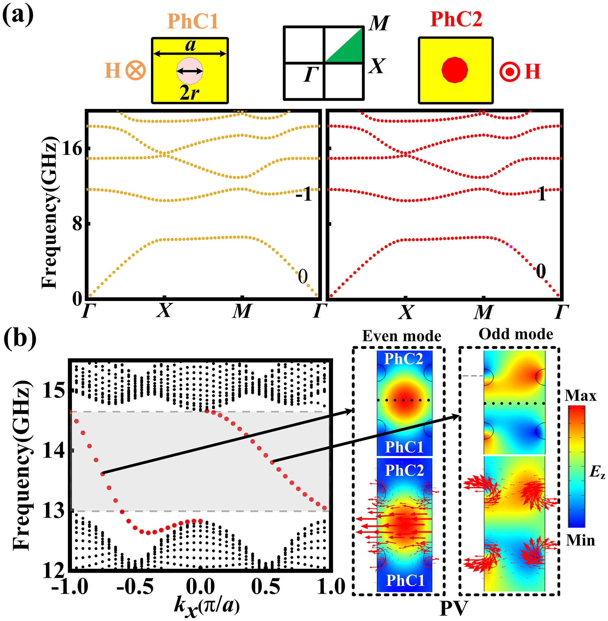
    Fig. 1. Band diagrams of the topological PhC. (a) Upper panel, unit cell of PhC1 and PhC2 with opposite biasing magnetic fields. The inset shows the first Brillouin zone. Lower panel, band diagrams for PhC1 and PhC2, respectively. (b) Projected band diagrams for a supercell composed of 10-unit cells of both PhC1 and PhC2. Topological one-way edge states, represented by two red dashed lines, are marked in the shaded area. The electric field intensity Ez and Poynting vector of two edge states (left side, even mode; right side, odd mode) are confined at the interface of PhC1 and PhC2.
    Configuration of the waveguide system composed of the classical waveguide, transition waveguide, and topological waveguide. Region I is a conventional rectangular waveguide. Region II is a taper dielectric waveguide with partial metal cover. Region III is a topological waveguide channel formed by the domain wall of PhC1 and PhC2. The pentagram with different colors represents the β points corresponding to different positions x.
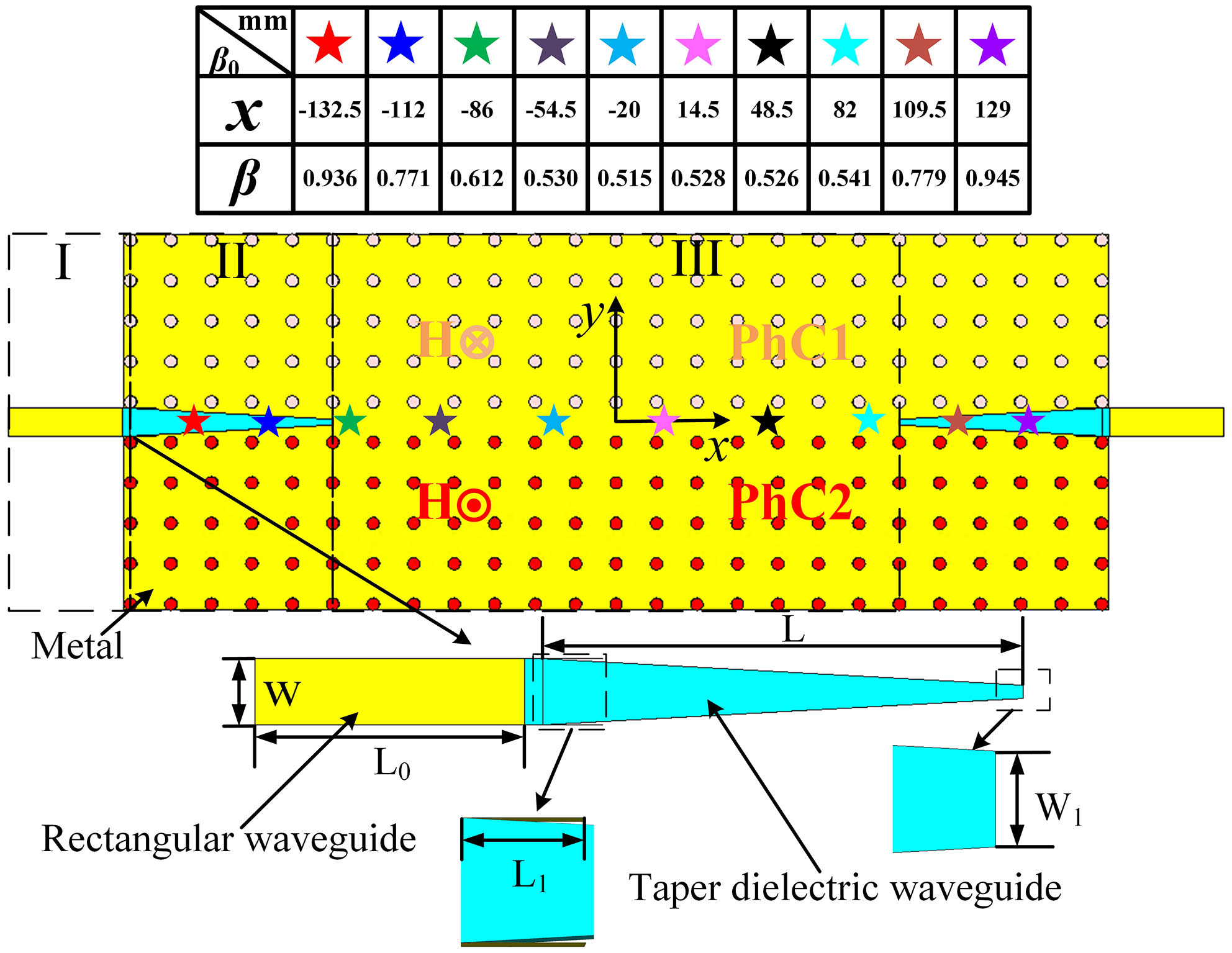
    Fig. 2. Configuration of the waveguide system composed of the classical waveguide, transition waveguide, and topological waveguide. Region I is a conventional rectangular waveguide. Region II is a taper dielectric waveguide with partial metal cover. Region III is a topological waveguide channel formed by the domain wall of PhC1 and PhC2. The pentagram with different colors represents the β points corresponding to different positions x.
    Design and analysis of taper transition structure. (a) Electric-force lines distribution in the x–z plane and guided wavelength λg in topological waveguide; (b) transition hybrid waveguide with gradually varied filled dielectric width w and the distribution of electric-force lines in the y–z plane; (c) matching mechanism of the propagation constant β in the topological waveguide at the central section and transition waveguides at the two ends; (d) wave phase at the x–z plane in the whole waveguide.
    Fig. 3. Design and analysis of taper transition structure. (a) Electric-force lines distribution in the x–z plane and guided wavelength λg in topological waveguide; (b) transition hybrid waveguide with gradually varied filled dielectric width w and the distribution of electric-force lines in the y–z plane; (c) matching mechanism of the propagation constant β in the topological waveguide at the central section and transition waveguides at the two ends; (d) wave phase at the x–z plane in the whole waveguide.
    Simulation and measurement of the whole waveguide system. (a) Simulated magnetic force line distribution in the waveguide; (b) photograph of the fabricated waveguide system and measurement setup; (c) Ez field distribution on the x–y plane at 13.5 GHz when EM energy is input from port1 (upper subfigure) and port2 (lower subfigure), respectively; (d), (e) measured and simulated S parameters of the whole waveguide when EM energy is input from (d) port1 and (e) port2.
    Fig. 4. Simulation and measurement of the whole waveguide system. (a) Simulated magnetic force line distribution in the waveguide; (b) photograph of the fabricated waveguide system and measurement setup; (c) Ez field distribution on the x–y plane at 13.5 GHz when EM energy is input from port1 (upper subfigure) and port2 (lower subfigure), respectively; (d), (e) measured and simulated S parameters of the whole waveguide when EM energy is input from (d) port1 and (e) port2.
    Robust transport of topological EM waves. (a)–(c) Ez field distribution in the x–y plane at 13.5 GHz, with (a) defects, (b) obstacle, and (c) randomness, respectively, when EM energy is input from port1; (d)–(f) simulated and measured S parameters of the whole waveguide corresponding to (a)–(c), respectively; (g) comparison of simulated S parameters for waveguides of defective, obstacle, random, and normal cases.
    Fig. 5. Robust transport of topological EM waves. (a)–(c) Ez field distribution in the x–y plane at 13.5 GHz, with (a) defects, (b) obstacle, and (c) randomness, respectively, when EM energy is input from port1; (d)–(f) simulated and measured S parameters of the whole waveguide corresponding to (a)–(c), respectively; (g) comparison of simulated S parameters for waveguides of defective, obstacle, random, and normal cases.
    Jianfei Han, Feng Liang, Yulin Zhao, Xiao Ding, Xiangru Wang, Deshuang Zhao, Bing-Zhong Wang. Highly efficient conversion from classical guided waves to topological chiral edge states[J]. Chinese Optics Letters, 2024, 22(2): 023902
    Download Citation