【AIGC One Sentence Reading】:A conversion structure for efficient coupling of classical waves to topological chiral edge states is proposed, enhancing transmission efficiency and paving the way for integrated topological devices.
【AIGC Short Abstract】:This study presents an efficient conversion method from classical guided waves to topological chiral edge states, mimicking the quantum Hall effect. A tapered transition design ensures high coupling efficiency and transmission in the microwave frequency. Simulation and measurement validate the approach, paving the way for integrated topological and classical devices with enhanced performance and reliability.
Note: This section is automatically generated by AI . The website and platform operators shall not be liable for any commercial or legal consequences arising from your use of AI generated content on this website. Please be aware of this.
Abstract
Electromagnetic topological chiral edge states mimicking the quantum Hall effect have attracted a great deal of attention due to their unique features of free backscattering and immunity against sharp bends and defects. However, the matching techniques between classical waveguides and the topological one-way waveguide deserve more attention for real-world applications. In this paper, a highly efficient conversion structure between a classical rectangular waveguide and a topological one-way waveguide is proposed and demonstrated at the microwave frequency, which efficiently converts classical guided waves to topological one-way edge states. A tapered transition is designed to match both the momentum and impedance of the classical guided waves and the topological one-way edge states. With the conversion structure, the waves generated by a point excitation source can be coupled to the topological one-way waveguide with very high coupling efficiency, which can ensure high transmission of the whole system (i.e., from the source and the receiver). Simulation and measurement results demonstrate the proposed method. This investigation is beneficial to the applications of topological one-way waveguides and opens up a new avenue for advanced topological and classical integrated functional devices and systems.
The photonic topological insulator (PTI) is the electromagnetic (EM) analogy of the topological insulator in electronic systems. PTI has attracted a great deal of attention due to the topologically protected one-way transport of edge states[1–4]. PTI can be constructed by mimicking the quantum Hall effect[4–11], the quantum spin Hall effect[12–17], or the quantum valley Hall effect[18–26] in electronic systems. In the quantum Hall effect system, the time reversal symmetry is broken through external magnetic fields, and the one-way edge state has the best robustness when encountering defects. Robust unidirectional backscattering-immune topological chiral edge states have been well demonstrated in PTIs based on gyromagnetic photonic crystals (PhCs) under biasing magnetic fields[4–11]. However, the coupling efficiency between an excitation source and the topological one-way waveguide and the matching techniques between classical waveguides and the topological one-way waveguide have not been studied well[27]. Since the edge states only exist on the domain wall, the topological one-way waveguide usually has nearly zero width, and hence it is essentially not compatible with conventional waveguides, which usually have a nonzero width. As the cornerstone of applications of these chiral edge states, matching methods between the conventional waveguide and the reflection-free topological one-way waveguide, or highly-efficient coupling techniques between excitation source and the topological one-way waveguide deserve more attention.
The highly efficient conversion structures between conventional guided waves and spoof surface plasmon polariton (SSPP) waves[28] and one-dimensional line waves[29] have been proposed. However, the propagations of these SSPP waves and line waves are not topologically protected (i.e., defects along the waveguide can lead to reflection and transmission loss). Recently, coupling from the classical transmission line modes to the topological modes based on the quantum spin Hall system[30], and coupling from the conventional waveguide modes to the topological modes based on the quantum valley Hall system[31] have been reported. Compared with quantum spin and quantum valley Hall systems, the topological modes based on the quantum Hall system have the strongest robustness against defects, which provides a powerful platform for the discovery and application of novel topological phenomena. Therefore, it is of great significance to study the effective coupling between conventional waveguide modes and the topological chiral edge states in the photonic quantum Hall system. However, to the best of our knowledge, how such topological modes interact with classical EM modes has not been reported. In previous work, usually point source (coaxial probe) excitations were used and reference planes were placed with a deviation from the excitation positions to measure the transmission rates[6–11]. In those situations, only a small part of the energy is coupled into the topological waveguide, resulting in low transmission efficiency, considering the whole system from source to receiver. This can be attributed to the mismatch of momentum and impedance between the two modes, resulting in relatively low conversion efficiency. Although ignoring the coupling efficiency between the source and the topological waveguide can verify the nontrivial topological physics, it is not enough for practical applications where a high system transmission rate is desired.
In this work, we report a highly efficient conversion method from classical guided waves to topological chiral edge states in magnetic photonic crystals. The main contributions of this work are summarized as follows. (1) We construct a domain wall waveguide channel supporting topological chiral edge states in the quantum Hall system, which consists of two kinds of distinct magnetic photonic crystal cells (i.e., PhC1 and PhC2). Chiral edge states can propagate along the topological waveguide channel when opposite external magnetic fields are applied in PhC1 and PhC2 regions to generate different topological phases. (2) We proposed a smooth tapered bridge that is a dielectric waveguide with partial metal covers to match the propagation constant and impedance of the conventional and the topological waveguides. The work mechanism of the proposed conversion structure is explained, and the transmission performances are demonstrated. (3) The high-efficiency transmission performance of the proposed configuration is robust and unaffected by defects, obstacles, and randomness.
Sign up for Chinese Optics Letters TOC. Get the latest issue of Chinese Optics Letters delivered right to you!Sign up now
2. Results and Discussions
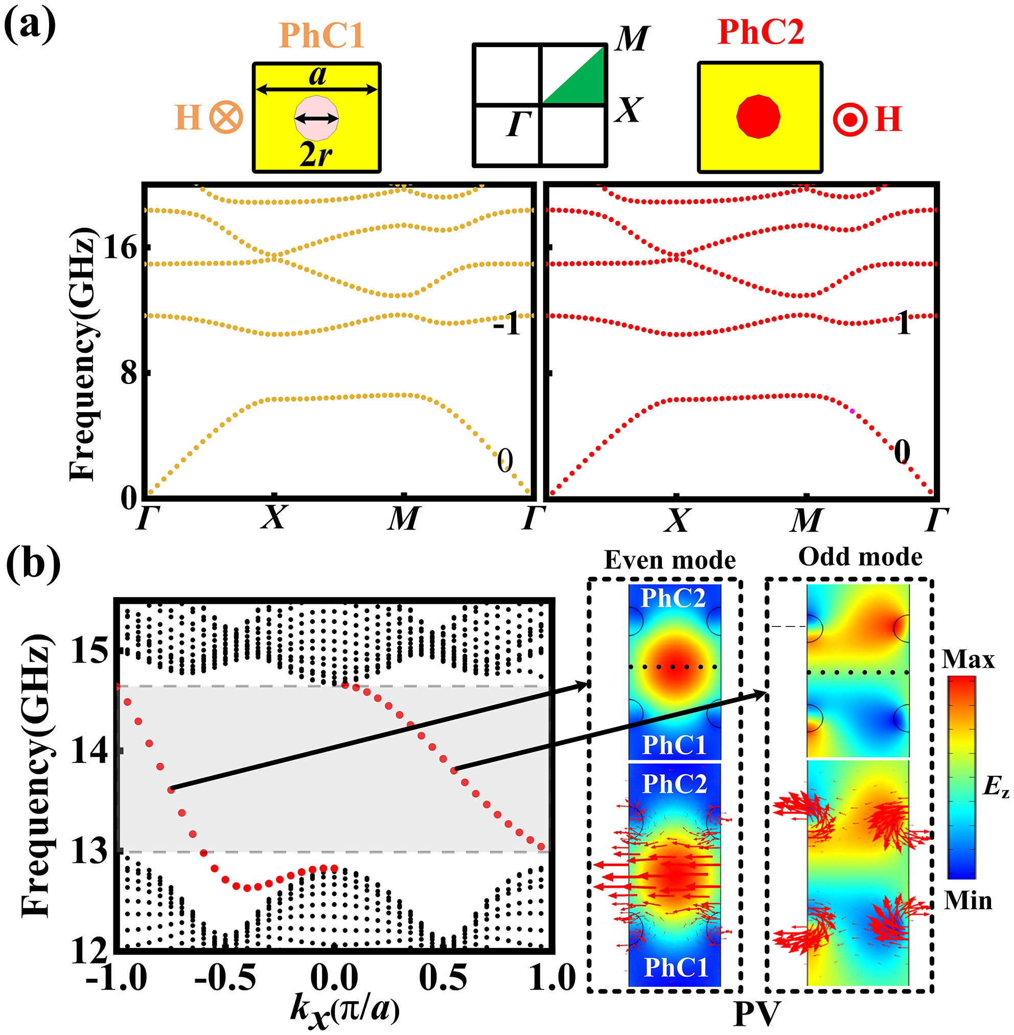
Topological edge states can usually be supported at the domain wall of PhCs with distinct topological properties. As illustrated in Figs. 1 and 2, the Chern PTI is composed of two domains, denoted by PhC1 and PhC2, made up of square lattice array of YIG rods under negative and positive -directional external magnetic fields, respectively. The lattice constant is . The diameter and height of each YIG rod are and , respectively. Here, the transverse magnetic (TM) modes of the 2D model are assumed. In this situation, the electric field has only the out-of-plane component (i.e., the component). The band structures of the magnetic PhCs can be simulated using commercial solver COMSOL Multiphysics. Figure 1(a) shows the simulated band structure for PhC1 and PhC2. Since the time-reversal symmetry is broken by the biased magnetic field, the PhC1 and PhC2 carry opposite Chern numbers in their second band. According to the bulk-edge correspondence, topological chiral edge states can be supported at the domain wall of the PhC1 and PhC2.
Figure 1.Band diagrams of the topological PhC. (a) Upper panel, unit cell of PhC1 and PhC2 with opposite biasing magnetic fields. The inset shows the first Brillouin zone. Lower panel, band diagrams for PhC1 and PhC2, respectively. (b) Projected band diagrams for a supercell composed of 10-unit cells of both PhC1 and PhC2. Topological one-way edge states, represented by two red dashed lines, are marked in the shaded area. The electric field intensity Ez and Poynting vector of two edge states (left side, even mode; right side, odd mode) are confined at the interface of PhC1 and PhC2.
Figure 2.Configuration of the waveguide system composed of the classical waveguide, transition waveguide, and topological waveguide. Region I is a conventional rectangular waveguide. Region II is a taper dielectric waveguide with partial metal cover. Region III is a topological waveguide channel formed by the domain wall of PhC1 and PhC2. The pentagram with different colors represents the β points corresponding to different positions x.
A supercell composed of 10 unit cells of both PhC1 and PhC2 is established to further analyze the property of the topological edge states. The projection bands of the supercell are shown in Fig. 1(b). Topological edge modes and bulk modes are labeled with red dotted lines and black dotted lines, respectively. Only two topological one-way edge states (i.e., the even mode and the odd mode) can be found in the shaded region of the bulk bandgap. The distribution of Poynting vector (PV) and field intensity show that the EM energy is well confined at the domain wall of PhC1 and PhC2. This implies that topological chiral edge states can propagate along the one-dimensional topological waveguide composed of the domain wall of PhC1 and PhC2.
Figure 2 shows the configuration of the whole transmission system. It contains a conventional dielectric filled rectangular waveguide (Region I in Fig. 2) with a coaxial excitation, a topological one-way waveguide made of YIG rod array (Region III), and a transition structure (Region II) between them. The proposed transition structure is made from a tapered dielectric waveguide with a partial metal cover inserted into the YIG rod array. The transition structure works to achieve a smooth conversion from classical guided waves to topological edge states.
To make the topological one-way waveguide, we use gyromagnetic PhCs made from YIG rods with a relative permittivity and a dielectric loss tangent . The measured saturation magnetization is Gauss, and the ferromagnetic resonance linewidth is 10 Oe. In the absence of an external magnetic field, gyromagnetic characteristics can often be neglected. YIG is applied with a biased magnetic field in the out-of-plane ( axis) direction.
Region I is a conventional dielectric-filled rectangular waveguide fed by a coaxial probe with 50 Ω characteristic impedance. The width, height, length, and the relative permittivity of the filling dielectric of the rectangular waveguide are defined as , , , and , respectively. To match the propagation constants of the topological chiral edge states and the guided waves ( modes) in a rectangular waveguide, we propose a smooth tapered transition that generates gradient propagation constants, as shown in Region II of the configuration in Fig. 2. The transition is a tapered dielectric waveguide with a partial metal cover, where the total transition length is , the length of the metal cover is , and the gradient width varies from to , as shown in the zoomed-in plot in Fig. 2. In the transition, the tapered dielectric waveguide is designed to overcome the large mismatch in propagation constants and impedances between rectangular waveguides and topological waveguides. Therefore, it is necessary to make the propagation constant gradually vary from the rectangular waveguide to the topological waveguide. Note that since the tapered dielectric waveguide is inserted into the YIG array (PhC), Region II in Fig. 2 is actually a hybrid waveguide composed of the tapered dielectric waveguide and part of the PhC topological waveguide.
To gain insight into the matching mechanism, the variation of propagation constant along the propagation direction () from the left transition waveguide to the topological waveguide and then to the right transition waveguide is carefully investigated. As a comparison, first, a monopole antenna is used as a feed source without the matching structure, and the excited signal is directly coupled into the topological waveguide. The chiral edge state can transmit along the topological waveguide. The simulated electric-force line distribution on the plane at 13.5 GHz is plotted in Fig. 3(a). From this field distribution, we measure the guided wavelength of the edge state. Therefore, the propagation constant in the topological waveguide can be calculated from the guided wavelength of the edge state. It can be seen that in order to achieve high-efficiency transmission of topological chiral edge states, we should design a tapered bridge with a larger propagation constant than that in the topological waveguide. Next, the transition hybrid waveguide is designed and analyzed; its top view and side view are shown in Fig. 3(b), in which the dielectric-filled width is marked with a red line. The plane electric-force line distribution of the hybrid waveguide is obtained via full-wave simulation at 13.5 GHz, which is shown in the right panel in Fig. 3(b). Additionally, the tapered transition is divided into several sections with different widths , and the propagation constant of each section is obtained by analyzing the hybrid waveguide. Dispersion diagrams of each hybrid waveguide section with different dielectric widths are investigated by eigenmode simulations, and the propagation constants are then extracted at 13.5 GHz. The propagation constants of the transition waveguide and topological waveguide at different positions along the direction at 13.5 GHz are shown in Fig. 3(c), marked by the blue solid line. We can find that a perfect propagation constant (momentum) matching is obtained by using the tapered transition, where gradually changes from 0.93 to with increasing . Here, , and is the propagation constant of the hybrid waveguide with width .
Figure 3.Design and analysis of taper transition structure. (a) Electric-force lines distribution in the x–z plane and guided wavelength λg in topological waveguide; (b) transition hybrid waveguide with gradually varied filled dielectric width w and the distribution of electric-force lines in the y–z plane; (c) matching mechanism of the propagation constant β in the topological waveguide at the central section and transition waveguides at the two ends; (d) wave phase at the x–z plane in the whole waveguide.
In order to further demonstrate the validity of the proposed design and analysis, we perform a full-wave simulation on the whole matched waveguide and extracted the phase in the cross section, as shown in Fig. 3(d). The average propagation constant is extracted by the phase shift over a certain distance, marked by the red dots in Fig. 3(c). Evolution of with respect to position in the waveguide channel, where the coordinates are marked by the pentagram, is shown in Fig. 2. By comparison, we can find that the propagation constants obtained from eigenmode analysis and from full-wave simulation have good consistency. Moreover, it is demonstrated that the propagation constant is gradually varying from a conventional rectangular waveguide to a topological waveguide, which means that momentum matching is obtained via the transition structure.
To demonstrate the smooth transition from guided waves to topological chiral edge states, the whole waveguide structure is simulated by using the commercial software CST Studio Suite. The design was also fabricated and measured by using a vector network analyzer. Figure 4(a) shows the simulated field distribution in the plane in the waveguide. We note that the EM energy in the rectangular waveguide is smoothly coupled into the topological waveguide by the tapered transition when the dielectric width gradually decreases from to . Due to the bandgap-confined EM waves of PhCs, there is some energy leaky into the bulk region, but most of the EM energy is tightly confined on the dielectric waveguide and finally converted into edge states. Next, we demonstrate the one-way transmission feature of the waveguide. When the EM energy is input from the left port (port1), the topological edge state is excited and efficiently transmitted to the right port (port2) of the topological waveguide, as shown in Fig. 4(c), where distribution at 13.5 GHz is depicted. However, when the EM energy is input from the right port (port2), the EM energy transmission in the topological waveguide is prohibited, as shown in Fig. 4(d). Strong nonreciprocal isolation properties can also be observed at other frequencies in the topological waveguide.
Figure 4.Simulation and measurement of the whole waveguide system. (a) Simulated magnetic force line distribution in the waveguide; (b) photograph of the fabricated waveguide system and measurement setup; (c) Ez field distribution on the x–y plane at 13.5 GHz when EM energy is input from port1 (upper subfigure) and port2 (lower subfigure), respectively; (d), (e) measured and simulated S parameters of the whole waveguide when EM energy is input from (d) port1 and (e) port2.
To confirm the above simulation results, a prototype of the proposed waveguide is fabricated, as shown in Fig. 4(b). There are five layers along the and directions in the PhC1 and PhC2 domains, which are sufficient to present the bandgap characteristics of the periodic structure. YIG is arranged in the air according to a square lattice, as shown in Figs. 2 and 4(b). Transmission and isolation characteristics are described by simulated and measured parameters. A vector network analyzer is used for transmission measurements, which supports EM waves with frequency range from 300 kHz to 20 GHz. Figure 4(d) shows the parameters in the two cases (forward and backward), where the solid and dashed lines represent the simulation and measurement results, respectively. and correspond to the reflection coefficients in the forward and backward situations, which are lower than from 13 to 14 GHz. with higher than and with lower than correspond to the transmission coefficients in the forward and backward cases, which have a difference of 30–40 dB from 13 to 14 GHz. From the above results, we can find that due to the precision-uncontrollable experimental details, the measurements will inevitably deviate from the simulations, but they both reveal the nonreciprocal transport from 13 to 14 GHz. The simulation and measurement results are consistent with band theory expectations in Fig. 1(b). Therefore, these results provide strong evidence for one-way transmission in the topological waveguide. It should be noted that the measured transmission rates are a little smaller than the simulated ones, and the transmission loss mainly comes from subtle experimental control (e.g., the assemble error of YIG array) and sample manufacturing errors. Furthermore, the difference between the simulated and measured results is related to the actual nonuniform magnetic field bias on the YIG. Since there is a certain distance between the two permanent magnets in the measurement, on the one hand, the magnetic field strength attenuates along the YIG axis, and the bias on the YIG is inhomogeneous. On the other hand, the strength of the magnetic field generated by the permanent magnet may be different than that used in our simulation (i.e., ). Therefore, the operating bandwidth and transmission efficiency of the topological waveguide are affected by the nonuniform bias magnetic field compared with the simulation.
It is well known that the transmission of topological edge states is robust against various defects and perturbations. To verify the immunity of the proposed highly efficient topological waveguide to structural perturbations, we introduce three different structural perturbations [i.e., PEC plate (obstacle), metal pillars (defects), and larger area disorder (randomness)]. Figure 5 shows the field distribution and parameters at 13.5 GHz when EM energy is input from port1. In Figs. 5(a) and 5(b), the metal pillar and the PEC slab are marked by the black rectangular wire frame. It can be clearly seen from the electric field intensity distribution that the topological chiral edge states can bypass the metal plate and the metal pillar and continue to transport forward. After passing through the region with metal pillars or PEC plate, the edge states are almost completely recovered, which is nearly identical to the case without perturbation, depicted in Fig. 4(c). It is demonstrated that the PEC plate and metal pillars have little impact on the transmission of the topological chiral edge states. Next, we study the transmission of the edge states in the presence of large-area disorder in the PhC1 and PhC2 domains. Here, YIG rods without biased magnetic field (depicted by green color) were randomly assigned between the PhC1 and PhC2 domains marked by the rectangular wire frame. It can be seen from Fig. 5(c) that when large-area disorder is introduced, it can hardly prevent wave transmission due to the topologically protected feature. The proposed topological waveguide has excellent transmission and reflection-free properties, which provides useful guidelines for bridging between classic guided waves and topological one-way waves.
Figure 5.Robust transport of topological EM waves. (a)–(c) Ez field distribution in the x–y plane at 13.5 GHz, with (a) defects, (b) obstacle, and (c) randomness, respectively, when EM energy is input from port1; (d)–(f) simulated and measured S parameters of the whole waveguide corresponding to (a)–(c), respectively; (g) comparison of simulated S parameters for waveguides of defective, obstacle, random, and normal cases.
The simulated and measured parameters for the three types of configurations are shown in Figs. 5(d)–5(f). It is worth noting that the transmission and reflection coefficients and in Figs. 5(d) and 5(e) are almost the same as those of the undisturbed waveguide in Fig. 2. The robustness of one-way transport of the topological edge state stems from breaking the time-reversal symmetry, which is very different from valley edge state transport by breaking the symmetry of inversion. Due to the existence of backscattering channels in valley transmission that destroy the symmetry of inversion, transmission may be seriously deteriorated through wavelength-sized defects. In our design, almost all EM energy input from port1 can be transported to port2. The situation when EM energy is input from port2 is the same as that shown in Fig. 4(c). It is worth pointing out that the edge states can achieve high-efficiency transmission, even in the presence of perturbations. To more clearly show the transmission performance under different conditions, Fig. 5(g) shows the parameters of a PEC plate (obstacle), metal pillar (defect), and large-area disorder (randomness) compared with the undisturbed (normal) case. It can be seen that the transmission and reflection coefficients are almost the same in the four cases, which fully demonstrates the reflection-free feature of the edge states. Therefore, the time-reversal symmetry broken topological waveguide has strong robustness and also has the characteristics of highly efficient one-way transmission protected by topology and its reverse isolation. Though square lattice is used in this work, the proposed idea of momentum and impedance matching and mode conversion between classical guided waves and one-way topological edge states can be employed in other systems containing topological waveguides or devices made of magnetic PhCs. This work has potential applications in the integration of one-way topological waveguide systems and conventional waveguide systems.
3. Conclusion
In summary, we propose a highly efficient conversion design between classical waveguides and time-reversal symmetry broken topological waveguides for efficiently coupling an EM signal from an excitation source to the topological waveguide and efficiently extracting the signal from the topological waveguide to the receiver. The topological waveguide is composed of YIG PhC with opposite magnetic fields in its two domains. We use a rectangular waveguide as the conventional waveguide to feed the topological waveguide. Between the rectangular waveguide and the topological waveguide, we design a transition structure composed of a tapered dielectric waveguide with a partial metal cover. The transition structure can efficiently convert classical guided waves to topological chiral edge states due to the matching of momentum and impedance. To verify the excellent transmission performance, we fabricate the proposed waveguide. Both simulation and measurement results show that the transition structure can obviously improve the coupling between the excitation source and the topological waveguide and improve the transmission rate of the whole system. The difference between forward and backward transmission coefficients is about 30–40 dB, which demonstrates the one-way transport feature. We also demonstrate that the waveguide system has strong robustness against defects, obstacles, and randomness. This work provides useful insights and routines for designing practical topological and conventional integrated functional devices and systems.
 AI Video Guide
  AI Picture Guide
 AI One Sentence