
Shaojie Li, Peide Han. Effects of high temperature annealing and laser irradiation on activation rate of phosphorus[J]. Journal of Semiconductors, 2020, 41(12): 122701
- Journal of Semiconductors
- Vol. 41, Issue 12, 122701 (2020)
Abstract
1. Introduction
As is known, after annealing at a certain temperature for a certain time, the implanted impurities may undergo a large extent of redistribution in the solid, and the normal solid-state diffusion is negligible at this time. This effect has been observed in several substances implanted into silicon, such as boron[
How do you further improve the activation rate of phosphorus under the optimal annealing temperature? This has important guiding significance for further improving the efficiency of crystalline silicon solar cells and applying it to industrial production. Femtosecond (fs) laser irradiation is one of the most attractive manufacturing methods to produce black silicon (B-Si)[
2. Experimental section
2.1. Thermal annealing
In the experiment, P-type <100> silicon wafers with a resistivity of 1–10 Ω•cm were used. During the ion implantation, the samples oriented with their normal tilted 7° relative to the incident beam in order to avoid channeling effects. The silicon wafers were implanted with phosphorous at room temperature (energy = 55 keV, dose = 3 × 10 15 cm–2). Then these samples were isothermally annealed at various temperatures (800–950 °C) for 30 min in a nitrogen atmosphere.
After annealing, the electrochemical capacitance–voltage profiler (ECV) was used to measure the activated concentration, and the secondary ion mass spectroscopy (SIMS) was applied to measure the total concentration. Rutherford backscattering spectrometry (RBS) was used to measure the channel energy spectrum at different annealing temperatures.
2.2. Femtosecond laser irradiation
The samples were annealed at the temperature with the highest activation rate. Then they were irradiated by a femtosecond laser in vacuum. In order to obtain large-area samples, the vacuum cavity was mounted on a two-dimensional translation stage controlled by a computer program. The silicon wafers were moved in the S-line sweep at a rate of 1 mm/s.
Raman spectra was used to measure the crystallinity of the surface irradiated by the femtosecond laser. The ECV was applied to measure the activated concentration and the SIMS was used to measure the total concentration.
The ECV instrument used CVP21 produced by the French Wep Company, and NH4F/HF solution was used as the electrolyte. The instrument of SIMS was equipped with a CAMECA IMS-4F device using a 5-keV Cs beam. The experimental equipment for Rutherford backscatter analysis consists of a small particle accelerator, a vacuum target chamber, a particle detector, and electronic circuits. The accelerator provides He ions with 2 MeV energy and 4 to 5 nA, and the vacuum of the target chamber is 10–5 Pa. In this work, a Horiba Jobin–Yvon Raman system with a 488 nm laser was used to characterize all samples. Raman spectra were taken at room temperature with a monochromator equipped with a 600 lines/mm grating and excited power 2 mW. The light source used in the experiment of the femtosecond laser was a Ti:sapphire femtosecond laser amplifier (800 nm center wavelength, 120 fs pulse duration, and 1 kHz repetition rate).
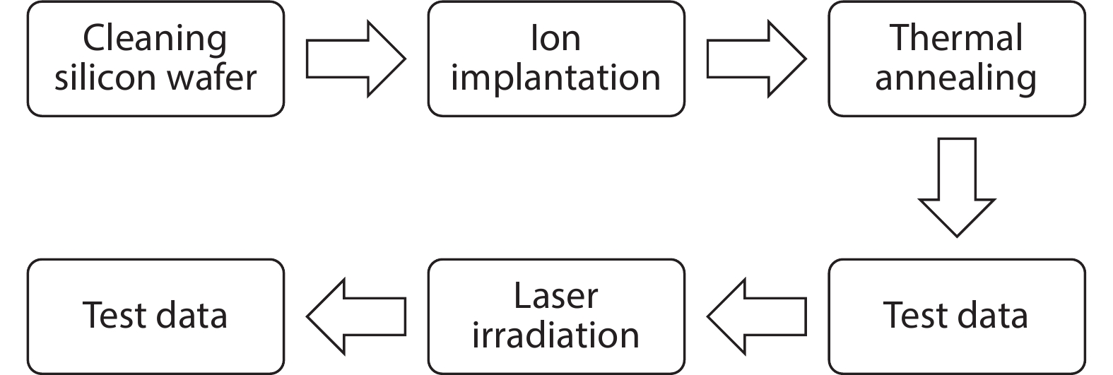
The experimental steps are shown in Fig. 1.
![]()
Figure 1.The experimental steps.
3. Results and discussion
Fig. 2(a) shows an image for the activation rate of phosphorus at different temperatures. The activation rate of phosphorus reached the highest under the condition of 850 °C. Fig. 2(b) exhibits that the areal density of phosphorus tested by ECV was the highest 850 °C, that is, the activated concentration of phosphorus measured at this temperature was the highest, which can explain the highest activation rate at 850 °C. Fig. 2(b) also shows that the areal density of phosphorus impurities before the junction depth of SIMS test was decreased with increasing temperature. The reason for this phenomenon is that as the temperature increases, more and more phosphorus impurities diffuse behind the junction depth. But the total phosphorus impurity concentration does not change. Fig. 2(c) shows the areal density of phosphorus impurities of the SIMS test, and it can fully illustrate this phenomenon.
![]()
Figure 2.(a) The activation rate of phosphorus at different temperatures. (b) Areal density of phosphorus of ECV and SIMS before the junction depth at different temperatures. (c) Areal density of phosphorus of SIMS at different temperatures.
The diffusion of high concentration phosphorus in silicon during annealing after implantation is a complex phenomenon. First, it is not only the substitution-interstitial (S-I) mechanism but also the vacancy mechanism that must be considered because of the high-concentration of phosphorus[
Fig. 3 shows the RBS images of ion implanted silicon wafers at different temperatures. It was observed that the interstitial impurities were the most at 850 °C. The experimental conditions for the number of interstitial impurities in the sample were as follows: 850 °C > 800 °C > 900 °C > 950 °C. If the interstitial impurities are mainly phosphorous interstitial impurities, RBS indicates that the activated concentration of phosphorus was the lowest at 850 °C, which is inconsistent with the measured data of ECV. If the interstitial impurities are mainly silicon interstitial impurities, it indicates that under the condition of 850 °C, the activated concentration of phosphorus was the highest, because the silicon in the interstitial impurities is mainly caused by the substitution of the phosphorus impurities. It is consistent with the maximum number of activated phosphorus impurities under the condition of 850 °C in the ECV measure. Therefore, interstitial impurities are mainly silicon interstitial impurities [
![]()
Figure 3.(Color online) RBS images at different temperatures.
The energy and yield of different elements are different after backscattering, which is reflected in different positions on the RBS[
Fig. 4(a) shows the measured results of ECV and SIMS at 850 °C. The activated concentration of phosphorus at the surface was the highest. As the depth was increased, the activated concentration was decreased. Fig. 4(b) shows the change of activation rate with depth at 850 °C. From Fig. 4(b), it can be seen that the activation rate showed a downward trend with the increase of the depth. It is verified that the diffusion after a certain depth in the process of thermal annealing is dominated by interstitial diffusion[
![]()
Figure 4.(Color online) (a) ECV and SIMS measured results at 850 °C. (b) The activation rate with thickness at 850 °C.
Why doesn't the activated phosphorus in the high-concentration area diffuse? A qualitative explanation is as follows[
In the process of deactivation in the high concentration area, it is assumed that the mobile (P-V)– reacts with the replacement phosphorus (
This reaction generates two I; and one I can be used to form a (P-V)-, the other interstitial silicon will remain. Therefore, this cycle generates one additional I. However, the resulting I will actually diffuse out of this area. If one of the two I, which are generated in the reaction, goes outside without reacting or vanishes at the surface, additional I cannot be expected in the high-concentration region. It is plausible that the rationality of I disappearing in a high concentration region or on the surface is more than 50%. Furthermore, if (P-V)– diffusion is outside the high-concentration area, it means that there is no enough I generation source, and there is no way to generate enough (P-V)–. This may explain that why the activated phosphorus does not diffuse in the high concentration area.
The femtosecond laser has ultra-high energy, and its interaction with matter is an instant process. The process of the femtosecond laser and the silicon surface is as follows: (1) the pulse energy is quickly deposited on the silicon surface within the femtosecond time scale; (2) the electrons absorb ultra-high pulse energy and rapidly warm up and ionize into electron gas; (3) the high energy electron gas transfers energy to surrounding “cold” atoms through electron–photon coupling in the order of picoseconds to achieve energy transfer[
Fig. 5 is the normalized Raman image under different energy-flux densities. The sample under the energy-flux density of 0.7 kJ/m2 had obvious background noise, but the Raman peak was only 520 cm–1, which means that under this energy-flux density, only the characteristic peak of crystalline silicon, but no amorphous peak was formed. This also showed that the surface has energy damage, which is, however, not enough to produce lattice distortion. In addition, except for the energy-flux density of 0.7 kJ/m2, the Raman spectra of the remaining energy-flux densities were almost the same, indicating that there is almost no damage to the surface under the remaining energy-flux densities. In order to ensure the crystallinity of the surface irradiated by femtosecond laser, the highest energy-flux density of laser irradiation was 0.65 kJ/m2.
![]()
Figure 5.(Color online) Raman spectra of samples under different energy-flux densities.
Fig. 6(a) shows an image of the activation rate of phosphorus under different energy-flux densities. The activation rate of phosphorus was almost the same under the energy-flux density of 0.3 kJ/m2 and without laser irradiation. With the increase of the energy-flux density (> 0.3 KJ/m2), the activation rate of phosphorus was increased. Under the energy-flux density of 0.65 KJ/m2, the activation rate of phosphorus was the highest. The activation rate of phosphorus was increased from 67% to 74.81%. Fig. 6(b) reveals the reason for the change in the activation rate of phosphorus is that the change in the activated areal density of phosphorus impurities after laser irradiation. The SIMS measured results demonstrated that laser irradiation did not change the distribution of phosphorus diffusion. Thus, the areal density of phosphorus impurities before the junction depth of the SIMS tested was basically a fixed value, about 2.82 × 1015 cm–2.
![]()
Figure 6.(a) The activation rate of phosphorus at different energy-flux densities. (b) Areal density of phosphorus of ECV and SIMS at different energy-flux densities.
It can be seen from Fig. 7(a) that with the increase of the energy-flux density, the activated concentration of phosphorus was increased, and in the tail region of the curve, the activated concentration of phosphorus was increased significantly. Fig. 7(b) shows the change of activation rate with thickness under different energy-flux densities. With the increase of energy-flux density, the activation rate of phosphorus at each thickness was increased, but the increase of the activation rate was mainly reflected at depths of more than 100 nm. Additionally, in the absence of laser irradiation, the activation rate was about 50% at about 100 nm. Thus, when the thickness of crystalline silicon is above 100 nm, interstitial impurities of phosphorus dominate[
![]()
Figure 7.(Color online) (a) ECV test results at different laser irradiation conditions. (b) Effective activation rate with thickness at different laser irradiation conditions.
A speculation was proposed that laser irradiation can increase the activation rate of phosphorus impurities.
At present, the model of the silicon surface irradiated by the femtosecond laser is widely accepted as the plasma model, that is, the silicon will not melt during the laser irradiation, but a superfluid is generated[
4. Conclusion
Annealing experiments were conducted at different temperatures on silicon samples after implantation of phosphorus ions (energy = 55 keV, dose = 3 × 1015 cm–2). The activation areal density of phosphorus impurities reached the highest at 850 °C. Simultaneously, the highest activation rate of 67% was obtained. This discovery is of great importance to the current industrial production. Yingli is now building a solar cell production line that uses ion implantation technology. This condition can be directly used in the production line. Experiments showed that the activated concentration of phosphorus at the surface was high. As the depth increases, the activated concentration was decreased, and the activation rate also was decreased.
When irradiating the samples with a femtosecond laser, the activation rate of phosphorus had a certain increase on the original basis. Without obvious damage to the sample surface, the activation rate of phosphorus was increased from 67% to 74.81%. This supported that the femtosecond laser can increase the activation rate of phosphorus. This provides a feasible method of improving the efficiency of crystalline silicon solar cells in the future.
Acknowledgements
This work was supported by National Key R&D Program of China (No. 2018YFB1500500). We thank Yingli Company and TEDA Institute of Applied Physics of Nankai University for their help in this research.
References
[1] W K Hofker. Implantation of boron in silicon. Philips Res Rep, 15, 189(1975).
[2] W Skorupa, E Wieser, R Groetzschel et al. High energy implantation and annealing of phosphorus in silicon. Nucl Instrum Methods Phys Res, 19/20, 335(1987).
[3] M A Kisielewicz. The damage-dependent atom and carrier profiles in phosphorus-implanted silicon. Thin Solid Films, 109, 11(1983).
[4] M Y Tsai, B G Streetman. Recrystallization of implanted amorphous silicon layers. I. Electrical properties of silicon implanted with BF+2 or Si++B+. J Appl Phys, 50, 183(1979).
[5] E Landi, S Guimaraes, S Solmi. Influence of nucleation on the kinetics of boron precipitation in silicon. Appl Phys A, 44, 135(1987).
[6] S Solmi, E Landi, F Baruffaldi. High-concentration boron diffusion in silicon: Simulation of the precipitation phenomena. J Appl Phys, 68, 3250(1990).
[7] P A Stolk, H J Gossmann, D J Eaglesham et al. Physical mechanisms of transient enhanced dopant diffusion in ion-implanted silicon. J Appl Phys, 81, 6031(1997).
[8] K Suzuki, Y Tada, Y Kataoka et al. Maximum active concentration of ion-implanted phosphorus during solid-phase epitaxial recrystallization. IEEE Trans Electron Devices, 54, 1985(2007).
[9] T Hadjersi. Annihilation kinetics of defects induced by phosphorus ion implantation in silicon. Appl Surf Sci, 185, 140(2001).
[10] C Wu, C H Crouch, L Zhao et al. Near-unity below-band-gap absorption by microstructured silicon. Appl Phys Lett, 78, 1850(2001).
[11] C H Crouch, J E Carey, M Shen et al. Infrared absorption by sulfur-doped silicon formed by femtosecond laser irradiation. Appl Phys A, 79, 1635(2004).
[12] J R Köhler, S J Eisele. Phosphorus out-diffusion in laser molten silicon. J Appl Phys, 117, 145701(2015).
[13] M T Winkler, D Recht, M J Sher et al. Insulator-to-metal transition in sulfur-doped silicon. Phys Rev Lett, 106, 51(2011).
[14] H B Normann, B G Svensson, E Monakhov. Formation of shallow front emitters for solar cells by rapid thermal processing. Phys Status Solidi, 9, 2138(2012).
[15] M Uematsu. Simulation of boron, phosphorus, and arsenic diffusion in silicon based on an integrated diffusion model, and the anomalous phosphorus diffusion mechanism. J Appl Phys, 82, 2228(1997).
[16] A Othonos. Probing ultrafast carrier and phonon dynamics in semiconductors. J Appl Phys, 83, 1789(1998).
[17] H Cerva. Comparison of transmission electron microscope cross sections of amorphous regions in ion implanted silicon with point-defect density calculations. J Electrochem Soc, 139, 3631(1992).
[18] M Uematsu. Implantation species dependence of transient enhanced diffusion in silicon. J Appl Phys, 83, 120(1998).
[19] E Schroer, M Uematsu. Simulation of clustering and pile-up during post-implantation annealing of phosphorus in silicon. Jpn J Appl Phys, 38, 7(1999).
[20] M Uematsu. Simulation of clustering and transient enhanced diffusion of boron in silicon. J Appl Phys, 84, 4781(1998).
[21] M Uematsu. Simulation of high-concentration phosphorus diffusion in silicon taking into account phosphorus clustering and pile-up. Jpn J Appl Phys, 38, 6188(1999).
[22]
[23] S K Sundaram, E Mazur. Inducing and probing non-thermal transitions in semiconductors using femtosecond laser pulses. Nat Mater, 1, 271(2002).
[24] P L Silvestrelli, A Alavi, M Parrinello et al. Ab initio molecular dynamics simulation of laser melting of silicon. Phys Rev Lett, 77, 3149(1996).
[25] H W Lo, A Compaan. Raman measurement of lattice temperature during pulsed laser heating of silicon. Phys Rev Lett, 44, 1604(1980).

Set citation alerts for the article
Please enter your email address
© Copyright 2018-2021 | Chinese Laser Press. All Rights Reserved 沪ICP备15018463号-20