
Dajian Liu, Long Zhang, Hexin Jiang, Daoxin Dai, "First demonstration of an on-chip quadplexer for passive optical network systems," Photonics Res. 9, 757 (2021)
- Photonics Research
- Vol. 9, Issue 5, 757 (2021)
Abstract
1. INTRODUCTION
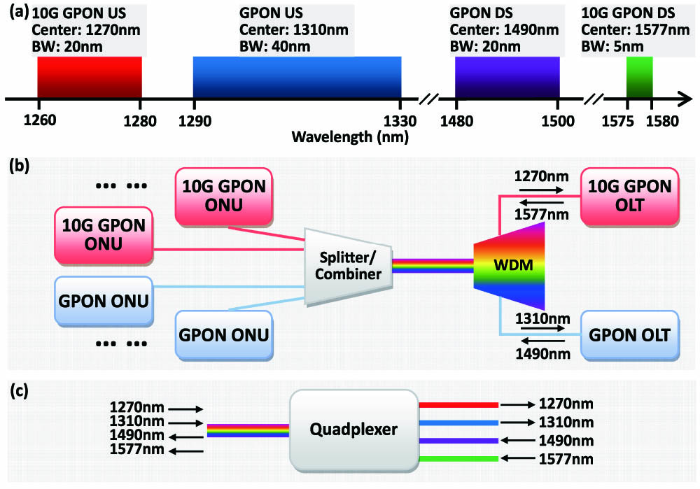
Figure 1.(a) PON wavelength plan. US, upstream; DS, downstream; BW, bandwidth. (b) PON configuration with the coexistence of GPON and 10G GPON. (c) Structure schematic diagram of a quadplexer.
As it is well known, silicon photonics has become very promising because of CMOS compatibility, low waveguide loss, and high integration density. Numerous silicon photonic devices have been demonstrated successfully for data transmission [5–9]. In particular, for PON systems, lots of special photonic components are needed [10–12], such as diplexers, triplexers [13–15], and quadplexers [16]. Among them, diplexers and triplexers have been developed successfully with silicon photonic technology in recent years. In contrast, it is still a big challenge to develop on-chip quadplexers due to the special requirements for the wavelengths as well as the bandwidths of the four channels. To the best of our knowledge, no on-chip quadplexer has been reported yet.
As shown in Figs. 1(a)–1(c), a quadplexer is proposed to realize the co-existence of GPON and 10G GPON by combining the two channels of 1270/1310 nm for downloading and the two channels of 1490/1577 nm for uploading. The corresponding bandwidths for these four channels are 20, 40, 20, and 5 nm, respectively. There have been several typical on-chip WDMs using for example, arrayed-waveguide gratings (AWGs) [17,18], etched diffraction gratings (EDGs) [19], microring resonators (MRRs) [20], and Mach–Zehnder interferometers (MZIs) [21,22]. According to the working principle, AWGs and EDGs are suitable for multichannel WDM systems with uniform channel spacing in a wavelength range limited by the free spectral range (FSR). Even though a novel cross-order silica AWG triplexer with three channels of 1310/1490/1550 nm was proposed to break the FSR limitation [18], it is still inflexible for AWGs/EDGs to achieve nonuniform bandwidths as desired for triplexers as well as the quadplexers considered in this paper. Similarly, WDMs based on cascaded MZIs do not have nonuniform channel spacing as desired and the wavelength range is also limited by the FSR. Furthermore, it usually requires critical control of the phase shifts and the coupling ratios for MZIs, which causes fabrication challenges. When using MRRs, designers can make the channel wavelengths flexible and the channel bandwidth is also flexible. However, the bandwidth is usually 1–2 nm or less and the FSR is only several tens of nanometers, according to the minimum bending radius. As a result, MRR-based WDMs also do not provide a channel bandwidth as wide as 5–40 nm and an operation wavelength range as wide as
In this paper, we propose and demonstrate what we believe, to the best of our knowledge, is the first on-chip quadplexer by using four cascaded multimode waveguide grating (MWG) filters. Previously, we realized a four-channel coarse wavelength division (de)multiplexer based on cascaded MWGs that works well in the 80 nm wide O-band covering the channels of 1271/1291/1311/1331 nm to satisfy the demands in short-distance optical interconnects (e.g., data centers) [23]. Recently, a silicon-based on-chip triplexer was also realized with three cascaded MWGs for the three channels of 1310/1490/1550 nm in fiber-to-the-home (FTTH) systems [24]. For the realized triplexer, the challenge is to design the MWGs carefully with optimized apodization strengths, corrugation depths, and periods, to achieve low losses and low cross-talk as well as the desired bandwidths of 100, 20, and 10 nm for the channels of 1310, 1490, and 1550 nm, respectively. In contrast, the design for the MWGs for the present on-chip quadplexer is even more challenging because of the ultrawide operation wavelength range covering the O-, S- and L-bands (i.e., 1270/1310/1490/1577 nm) and their nonuniform bandwidths of 20/40/20/5 nm. It means that one should carefully take the waveguide dispersion and the grating effects for more than one mode into account. Fortunately, four MWG-based filters were successfully designed with satisfactory performances. For the fabricated on-chip quadplexer, flat-top responses have been achieved with low excess losses of
Sign up for Photonics Research TOC. Get the latest issue of Photonics Research delivered right to you!Sign up now
2. STRUCTURE AND DESIGN
![]()
Figure 2.Schematic configurations: (a) proposed quadplexer; (b) MWG-based filter, consisting of a mode (de)multiplexer and an MWG-based filter; (c) mode (de)multiplexer based on an adiabatic dual-core taper; and (d) longitudinal apodization for the MWG.
For the first MWG-based filter operating with the channel of 1270 nm, the
![]()
Figure 3.(a) Calculated dispersion curves of an SOI strip waveguide for the
Regarding the ultrawide working wavelength range for the quadplexer, two broadband
The grating structures are designed according to the phase-matching condition between the
![]()
Figure 4.Calculated transmittance spectra at the drop and through ports for the designed MWGs at the channels of (a) 1270, (b) 1310, (c) 1490, and (d) 1577 nm.
Figures 4(c) and 4(d) show the calculated spectral responses for the designed MWG-based filters for the channels of 1490 nm and 1577 nm, respectively. Their parameters are chosen as follows:
![]()
Figure 5.Simulated transmissions at the drop port of the designed MWG filter at the 1577 nm channel when assuming that there is some core-width variation (i.e.,
3. FABRICATION AND MEASUREMENT
![]()
Figure 6.(a) Microscope image of the fabricated quadplexers on silicon. SEM images of the grating couplers working around (b) 1300 nm and (c) 1530 nm, parts of gratings for (d) 1270 nm, (e) 1310 nm, (f) 1490 nm, and (g) 1577 nm.
![]()
Figure 7.Measured spectral responses for the four channels of (a) 1270 nm, (b) 1310 nm, (c) 1490 nm, and (d) 1577 nm.
![]()
Figure 8.(a) Measurement setup for the eye diagram, including tunable lasers, polarization controllers (PCs), Mach–Zehnder modulators (MZMs), pulse pattern generators (PPGs), an off-chip multiplexer (MUX), the device under test (DUT), an optical receiver (Recv.), and a digital communication analyzer (DCA). Measured eye diagrams for the channels of (b) 1271 nm, (c) 1311 nm, and (d) 1577 nm.
![]()
Figure 9.(a) Microscopy picture of the fabricated identical MWG-based filters; (b) measurement responses at the drop-port; (c) the central wavelength deviation and (d) the 3 dB bandwidth deviation among six samples.
4. SUMMARY AND DISCUSSION
In conclusion, in this paper we have proposed and realized a silicon-based, on-chip quadplexer for the first time, to the best of our knowledge. The quadplexer is designed with four cascaded MWG-based filters. In the present design, apodization gratings, grating tapers, and bent waveguides have been introduced to greatly reduce the cross-talk. All channels for the designed quadplexer have box-like responses with low excess losses (
References
[1] V. Houtsma, D. van Veen, E. Harstead. Recent progress on standardization of next-generation 25, 50, and 100G EPON. J. Lightwave Technol., 35, 1228-1234(2017).
[2] J. S. Wey. The outlook for PON standardization: a tutorial. J. Lightwave Technol., 38, 31-42(2020).
[3] D. Z. Zhang, D. K. Liu, X. M. Wu, D. Nesset. Progress of ITU-T higher speed passive optical network (50G-PON) standardization. J. Opt. Commun. Netw., 12, D99-D108(2020).
[4] T. Horvath, P. Munster, V. Oujezsky, N. H. Bao. Passive optical networks progress: a tutorial. Electronics, 9, 1081(2020).
[5] Y. T. Wan, S. Zhang, J. C. Norman, M. J. Kennedy, W. He, S. T. Liu, C. Xiang, C. Shang, J. J. He, A. C. Gossard, J. E. Bowers. Tunable quantum dot lasers grown directly on silicon. Optica, 6, 1394-1400(2019).
[6] D. Benedikovic, L. Virot, G. Aubin, J. M. Hartmann, F. Amar, X. Le Roux, C. Alonso-Ramos, E. Cassan, D. Marris-Morini, P. Crozat, F. Boeuf, J. M. Fedeli, C. Kopp, B. Szelag, L. Vivien. 40 Gbps heterostructure germanium avalanche photo receiver on a silicon chip. Optica, 7, 775-783(2020).
[7] J. Witzens. High-speed silicon photonics modulators. Proc. IEEE, 106, 2158-2182(2018).
[8] D. X. Dai, L. Liu, S. M. Gao, D. X. Xu, S. L. He. Polarization management for silicon photonic integrated circuits. Laser Photon. Rev., 7, 303-328(2013).
[9] D. X. Dai, J. E. Bowers. Silicon-based on-chip multiplexing technologies and devices for peta-bit optical interconnects. Nanophotonics, 3, 283-311(2014).
[10] J. Zhang, T.-Y. Liow, G.-Q. Lo, D.-L. Kwong. 10Gbps monolithic silicon FTTH transceiver without laser diode for a new PON configuration. Opt. Express, 18, 5135-5141(2010).
[11] L. Xu, Q. Li, N. Ophir, K. Padmaraju, L.-W. Luo, L. Chen, M. Lipson, K. Bergman. Colorless optical network unit based on silicon photonic components for WDM PON. IEEE Photon. Technol. Lett., 24, 1372-1374(2012).
[12] S. Straullu, P. Savio, G. Franco, R. Gaudino, V. Ferrero, S. Bernabe, M. Fournier, V. Muffato, S. Menezo, B. Charbonnier, E. Temporiti, D. Baldi, G. Minoia, M. Repossi, L. Carroll, J. Lee, P. O’Brien, R. Marchetti, G.-H. Duan, F. Saliou, S. Abrate. Demonstration of a partially integrated silicon photonics ONU in a self-coherent reflective FDMA PON. J. Lightwave Technol., 35, 1307-1312(2017).
[13] Y. C. Shi, J. Y. Chen, H. N. Xu. Silicon-based on-chip diplexing/triplexing technologies and devices. Sci. China Inform. Sci., 61, 080402(2018).
[14] J. Y. Chen, L. Liu, Y. C. Shi. A polarization-insensitive dual-wavelength multiplexer based on bent directional couplers. IEEE Photon. Technol. Lett., 29, 1975-1978(2017).
[15] H. H. Chang, Y. H. Kuo, R. Jones, A. Barkai, J. E. Bowers. Integrated hybrid silicon triplexer. Opt. Express, 18, 23891-23899(2010).
[16] . Gigabit-capable passive optical networks (G-PON): enhancement band(2018).
[17] S. H. Jeong, Y. Onawa, D. Shimura, H. Okayama, T. Aoki, H. Yaegashi, T. Horikawa, T. Nakamura. Polarization diversified
[18] X. F. Lin, T. T. Lang, J.-J. He. Design analysis and experimental verification of cross-order AWG triplexer based on silica-on-silicon. J. Lightwave Technol., 29, 1407-1413(2011).
[19] S. Pathak, P. Dumon, D. Van Thourhout, W. Bogaerts. Comparison of AWGs and echelle gratings for wavelength division multiplexing on silicon-on-insulator. IEEE Photon. J., 6, 4900109(2014).
[20] Y. Tan, D. X. Dai. Silicon microring resonators. J. Opt., 20, 054004(2018).
[21] H. N. Xu, L. Liu, Y. C. Shi. Polarization-insensitive four-channel coarse wavelength-division (de)multiplexer based on Mach-Zehnder interferometers with bent directional couplers and polarization rotators. Opt. Lett., 43, 1483-1486(2018).
[22] D. J. Liu, H. N. Xu, Y. Tan, Y. C. Shi, D. X. Dai. Silicon photonic filters. Microw. Opt. Technol. Lett., 1-17(2020).
[23] D. J. Liu, M. Zhang, Y. C. Shi, D. X. Dai. Four-channel CWDM (de)multiplexers using cascaded multimode waveguide gratings. IEEE Photon. Technol. Lett., 32, 192-195(2020).
[24] D. J. Liu, M. Zhang, D. X. Dai. Low-loss and low-crosstalk silicon triplexer based on cascaded multimode waveguide gratings. Opt. Lett., 44, 1304-1307(2019).
[25] D. X. Dai, C. L. Li, S. P. Wang, H. Wu, Y. C. Shi, Z. H. Wu, S. M. Gao, T. G. Dai, H. Yu, H. K. Tsang. 10-channel mode (de)multiplexer with dual polarizations. Laser Photon. Rev., 12, 1700109(2018).
[26] D. X. Dai, H. Wu. Realization of a compact polarization splitter-rotator on silicon. Opt. Lett., 41, 2346-2349(2016).


Set citation alerts for the article
Please enter your email address

© Copyright 2018-2021 | Chinese Laser Press. All Rights Reserved 沪ICP备15018463号-20