
Guo Tongchuang, Ren Yongjie, Lin Jiarui, Jin Yunchao, Zhang Zhenyu. Delay Compensation for Synchronization Signal in Rotating Laser-Scanning Measurement System[J]. Laser & Optoelectronics Progress, 2021, 58(3): 3120021
- Laser & Optoelectronics Progress
- Vol. 58, Issue 3, 3120021 (2021)
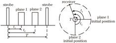
Fig. 1. Schematic of optical plane scanning
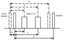
Fig. 2. Schematic of scanning time with delay
Fig. 3. Comparison of actual position and calculated position of receiver
Fig. 4. Schematic of synchronous optical circuit
Fig. 5. Schematic of delay trigger circuit
Fig. 6. Simulation waveforms of delay trigger circuit
Fig. 7. Flowchart of compensation algorithm
Fig. 8. Simulation waveforms of compensation algorithm
Fig. 9. Simulation waveforms with change of rotation speed
Fig. 10. Experimental scene. (a) Transmitting station measuring receiver; (b) oscilloscope measuring signal delay
Fig. 11. Comparison of measured time and theoretical time under different delays. (a) Plane 1; (b) plane 2
Fig. 12. Synchronous signal delay before and after compensation. (a) Before compensation ; (b) after compensation
|
Table 1. Delay of related devices
|
Table 2. Delay measurements of related devices
|
Table 3. Synchronous signal delay after adding delay
| |||||||||||||||||||||||||||||||||||
Table 4. Scanning time before and after compensation

Set citation alerts for the article
Please enter your email address
© Copyright 2018-2021 | Chinese Laser Press. All Rights Reserved 沪ICP备15018463号-20