Optical antennas have received considerable attention in recent years due to their unique ability to convert localized energy to freely propagating radiation and vice versa. Sidelobe level (SLL) is one of the most crucial parameters in antenna design. A low SLL is beneficial to minimize the antenna interference with other optical components. Here a plasmonic optical leaky-wave antenna with low SLL is reported. Shifting spatial frequency by periodically modulating the electric-field amplitude in a plasmonic gap waveguide enables a free-space coupled wave out of the antenna. At the same time, precise control of the aperture fields by the modulation depth allows for reducing SLL. Simulation results indicate that the proposed design can achieve a high directivity of 15.8 dB and a low SLL of at the wavelength of 1550 nm. A low SLL below is experimentally demonstrated within the wavelength range from 1527 to 1570 nm. In addition, the low-SLL property is further verified by comparing it with a uniformly modulated antenna. By modulating the guided waves in the plasmonic gap waveguide in different forms, the aperture fields can be flexibly arranged to achieve arbitrary wavefront shaping. It bridges the gap between guided and free-space waves and empowers plasmonic integrated devices to control free-space light, thus enabling various free-space functions.
1. INTRODUCTION
Future photonic circuits capable of high-speed data processing at optical frequencies depend on the nanoscale realization of highly efficient emitters and detectors at the nanoscale [1]. Similar to microwave and radio-frequency antennas, optical antennas can perform energy conversion between a guided-wave mode in optical waveguides and free-space radiation. With the rapid development of photonic integrated circuits in recent years, such nanostructures have attracted increasing attention for their wide range of applications, including sensing, optical wireless communications, light detection and ranging (LIDAR), and holography [2–5].
Dielectric gratings are one of the most common antennas in the optical band. Generally, periodic material perturbations embedded in these guided-wave structures are used to generate free-space radiation. On the other hand, surface plasmons are collective electronic oscillations localized to metal–dielectric surfaces, which can realize the manipulation of light below the diffraction limit [6]. As further miniaturization of photonic systems allows faster speeds and lower power levels in information processing and transport, various plasmonic-based optical devices have been extensively investigated [7,8], and plasmonic antennas are no exception. For example, simply referring to microwave antenna designs, various topologies have been put forward for optical nanoantennas, including V-shaped antennas [9], bow-Tie antennas [10], Yagi–Uda antennas [1,11,12], Vivaldi antennas [2], etc. However, most of these devices are designed for simply directing localized energy into free-space radiation. Precise control of antenna aperture fields allows us to modify the spatial radiation pattern and achieve various free-space functions. This strategy is usually adopted in leaky-wave antennas (LWAs), which feature gradual leakage of electromagnetic energy over the structure [13]. For example, aperture-coupling optical antenna arrays have also been developed for unidirectional radiation [14,15]. Properly arranging the radiation aperture, a highly directional beam can be generated in free space. In addition, sidelobe level (SLL), defined as the power density ratio in the strongest secondary lobe to that in the main lobe, is another important parameter characterizing antenna performance. A low SLL will significantly reduce interference between the antenna and other optical components in an optical integrated circuit, enabling high-density, large-scale integration.
Several approaches have been proposed to achieve low SLL, which can be divided into two categories according to the design strategy used. The first is the aperiodic spacing design (also known as sparse arrays), which is widely adopted in optical phased arrays to suppress the grating lobes caused by large element pitches [16,17]. Amplitude tapering is another way to reduce the antenna SLL. For example, an SLL below is achieved using a star coupler to generate a Gaussian amplitude distribution for the 64 channels of an optical phased array [18]. However, SLL reduction at the array level will hinder the miniaturization of communication systems. In Ref. [19], a Taylor amplitude distribution is applied to tailor the aperture fields of an LWA. Although a theoretical SLL of can be realized, the variation in the phase constant along the antenna makes it not ideal for generating highly directional beams.
Sign up for Photonics Research TOC. Get the latest issue of Photonics Research delivered right to you!Sign up now
An all-plasmonic optical LWA based on a plasmonic gap waveguide is developed here. In the presented design, periodic modulation of the guided waves by the gap width allows coupled waves out of the antenna. In contrast, the modulation depth controls the leakage factor for each period. By precisely designing the leaky constant to fulfill a Chebyshev amplitude distribution on the radiation aperture, a low SLL can be achieved accordingly. The simulation results indicate that the proposed all-plasmonic optical LWA can achieve a low SLL of and a high directivity of 15.8 dBi at 1550 nm. For the experimental demonstration, a low SLL below was experimentally measured within the wavelength range of 1527–1570 nm, while also exhibiting a low wavelength dispersion of 0.069 deg/nm. Finally, the SLL reduction of the proposed design is further verified by comparing it with the conventional structure. The proposed all-plasmonic LWA with low SLL, high directivity, and low dispersion would enable a variety of applications, especially for optical point-to-point wireless communications [20] and optical wireless links [21].
2. STRUCTURE AND DESIGN PRINCIPLE
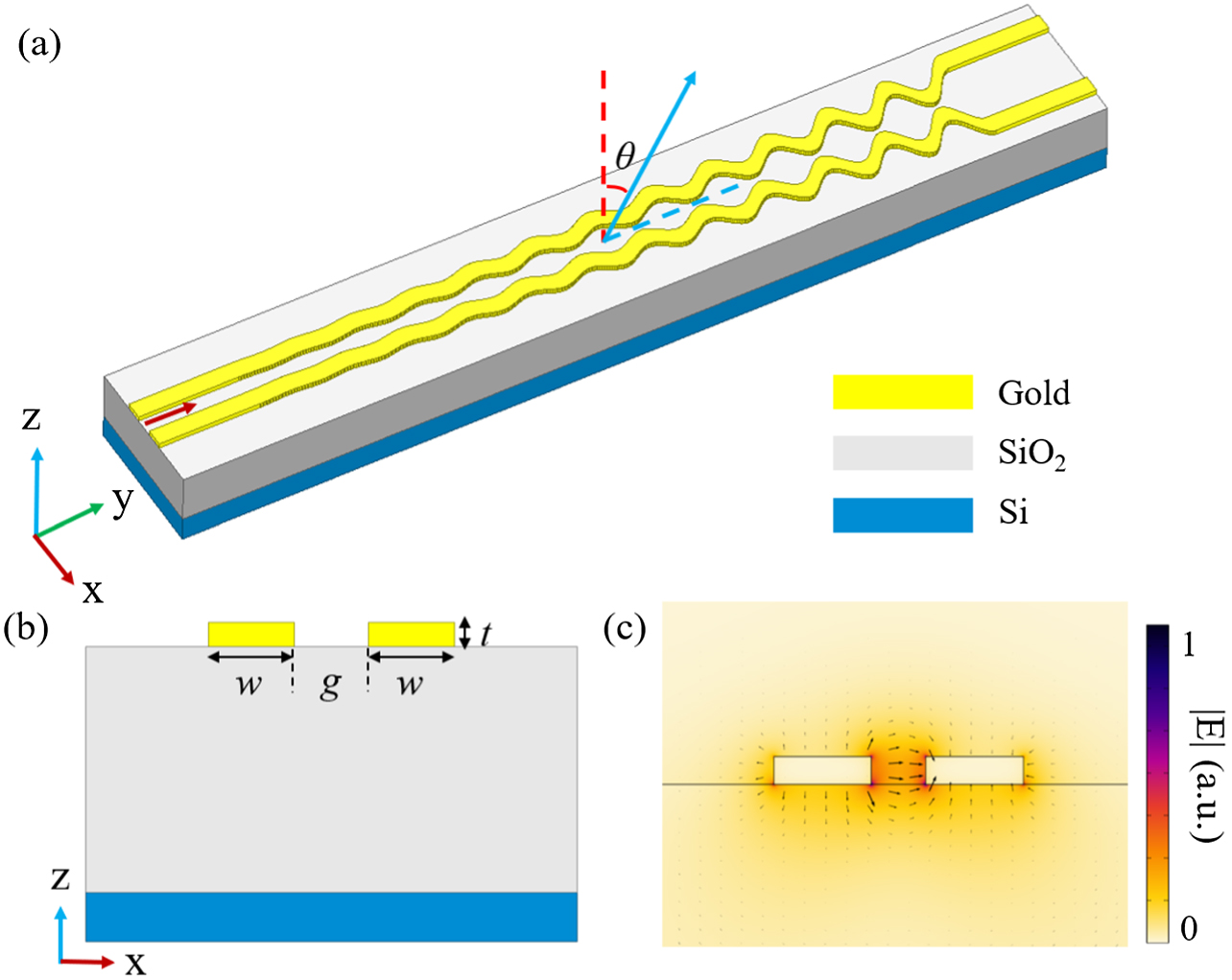
A schematic diagram of the proposed optical LWA is shown in Fig. 1(a). The antenna is composed of two identical gold strips on a glass substrate. The two strips with a width of and thickness of are separated by a gap , as shown in Fig. 1(b). A plasmonic gap waveguide is formed, and a highly confined plasmonic gap mode can be supported within it. The corresponding electric-field distribution of the mode is depicted in Fig. 1(c). By introducing a periodic modulation (e.g., sinusoidal variations) to the gap width, the guided-wave amplitude in the waveguide will be modulated accordingly, such that the guided waves can be converted to free-space radiation [22,23]. An additional design degree of freedom is added in the sinusoidal variation to complement the amplitude control of the aperture fields. A low SLL can be finally achieved by applying a Chebyshev amplitude distribution along the antenna radiation aperture.
Figure 1.(a) 3D schematic view of the proposed low-sidelobe plasmonic antenna. (b) Cross-section view of a uniform plasmonic gap waveguide. (c) E-field distribution of the plasmonic gap mode. The parameters are , , and .
For such a uniform plasmonic gap waveguide, a bounded guided wave is supported in the waveguide. It can be written as where is the amplitude constant, and is the complex wavenumber along the propagating direction, with and being the phase and attenuation constants, respectively. The bounded slow wave has the propagating constant ( is the free-space wavenumber). Thus, there is no coupling between the guided waves and free-space radiation mode. When periodic perturbation with a period of is introduced into the uniform structure, according to the Floquet mode theory, the modified wavenumber can be expressed as follows [24]: where represents the order of the corresponding Floquet mode and is an integer number. It suggests that parameter can flexibly adjust the wavenumber to make the bounded slow wave a fast wave satisfying , thus bridging the coupling between the guided wave and free-space radiation. The st Floquet mode is generally used to achieve the desired coupling. Therefore, the corresponding radiation angle of the far-field beam can be determined by
Sinusoidal variation employed in the gap width is responsible for coupling the energy in the guided-wave structure into free space. For conventional periodically modulated LWAs, the E-field intensity in guided-wave structures decays exponentially. The leakage factor is independently controlled by setting different modulation depths at each radiation period in this design to achieve the desired aperture field distribution. Since metals are highly lossy materials in the optical wavelength range, the overall attenuation constant of the structure is contributed jointly by the metal absorption loss and leakage factor , which can be expressed as . Therefore, the propagating loss of the guided-wave structure should be figured out first to control the leakage factor through different gap modulation depths.
A high-frequency structure simulator (HFSS) based on the finite element method (FEM) is used to investigate the properties of unmodulated and modulated plasmonic gap waveguides. The refractive indices of silicon and silica are set to 3.48 and 1.444, respectively. A Drude model describes the permittivity of gold in the near-infrared (IR) region with , , and [1].
The attenuation factor in a lossy system can be characterized by -parameters with a two-port transmission-line structure, as shown in Figs. 2(a) and 2(b). When the port reflection is ignored, it can be expressed as follows [25]: where represents the power transferred from port 1 to port 2. is the transmission line length. For a uniform gap plasmonic waveguide, the system loss is caused entirely by the metal absorption. A small unmodulated gap width means highly concentrated energy within the gap, resulting in higher metal absorption. The propagating loss decreases slightly with the increase of the gap width , as shown in Fig. 2(c).
Figure 2.Schematic views of (a) uniform plasmonic gap waveguide and (b) sinusoidally modulated antenna. (c) Metal absorption loss and normalized phase constant versus gap width . (d) Average attenuation constant of the system and leakage factor of the antenna as a function of modulation amplitude with .
The most attractive property of the structure is that the phase constant remains almost stable even within such a large variation range of from 360 to 600 nm. According to Eq. (3), Constant can guarantee a fixed radiation angle when modulating the gap width periodically, which will help generate a highly directional beam in the far field. The conventional antenna structure shown in Fig. 2(b) is used to obtain the desired leakage factor , where a sinusoidal modulation is introduced to the uniform plasmonic waveguide, resulting in additional radiation loss. In the modulation region, the gap width can be expressed as , where represents the modulation depth. The attenuation constant of the structure can be calculated by according to Eq. (4). A compromised propagating loss of 0.45 dB/μm is assumed for the guided waves in this structure for the sake of simplicity. Then, the corresponding leakage factor is calculated and plotted in Fig. 2(d). It can be seen that with a larger modulation depth, the st Floquet mode carries higher power, and the energy can be more easily radiated into free space, corresponding to a larger .
After clarifying the relationships between the leakage factor and modulation depth , the aperture amplitude of the LWA can be controlled arbitrarily. In the presented design, 12 radiated periods with a fixed modulation period μ are designed to realize a target SLL of , based on the Chebyshev amplitude distribution. The required amplitude distribution along the antenna radiation aperture is theoretically calculated and plotted in Fig. 3(a) (for design processes see Appendix A).
Figure 3.(a) Target Chebyshev amplitude distribution along antenna radiation aperture. (b) Theoretical modulation amplitudes and leakage factors for the 12 radiation periods. The blue symbols represent the fitting points with a quadratic function formula. (c) Simulated far-field patterns on the plane at 1500, 1550, and 1600 nm. (d) Radiation efficiency and directivity of the proposed LWA within the wavelength range of 1500 to 1600 nm.
The leakage factor of the th element can be expressed as [26] where is the desired amplitude distribution for the th element. is the total radiation periods of the design ( in our case). represents the system efficiency and is related to the metal absorption loss . The proposed LWA can be regarded as an array composed of a series of individual antenna elements. The efficiency is calculated for a radiation period with a propagation loss of 0.45 dB/μm. After the amplitude distribution along the antenna aperture is determined, the corresponding leakage factor for each period can be independently calculated by Eq. (5). According to the database in Fig. 2(d) (black curve), the desired modulation depth can be obtained by a mapping operation, as shown in Fig. 3(b).
The expression describing the gap width variation in the modulation region should be modified to implement the desired Chebyshev amplitude distribution along the antenna radiation aperture. A quadratic function formula is employed for the modulation coefficient , such that the gap width required for each radiation period can be fitted with a continuous geometry pattern. Therefore, assuming that the modulation region starts at , the gap width should have the following form: where , , and are the corresponding coefficients of the quadratic function. The following parameters are used to fit the theoretically designed values: , μ, and μ. The fitting values for all radiation periods are plotted in Fig. 3(b). It can be seen that the fitting values match well in the first several periods and slightly deviate from the theoretical design at the end. Since most of the energy has been dissipated in the first several radiation periods, even relatively large deviations of gap width in the subsequent periods will cause only slight amplitude variations of the aperture fields.
On the other hand, it is shown in Fig. 2(c) that the phase constant remains nearly constant with the gap width for a uniform plasmonic gap waveguide. A quadratic-function form is further adopted to increase the average gap width along the propagating direction for achieving a large modulation depth without intersecting the two gold strips. It does not affect the antenna radiation property. Therefore, the final form of the gap width can be expressed as where μ and μ. From Eq. (7), the proposed overall antenna structure can be constructed, as presented in Fig. 1(a). It should be noted that controls the guided-wave modulation amplitude, and thus determines the percentage of energy radiated from each antenna element. The Chebyshev amplitude distribution refers to aperture radiation fields, which indicates how much energy is radiated from each period. Therefore, the antenna’s desired aperture field amplitude distribution can be characterized by a series of leakage factors. Although the desired aperture amplitude features a symmetric distribution, considering that the LWA exhibits a gradual energy leakage along the guided-wave propagating direction, the modulated depth is a growing function with respect to the period number.
3D full-wave simulations were carried out to evaluate the performance of the designed device. In the simulations, a wave port feeds the waveguide and excites the desired plasmonic gap mode. An air box is set up one-quarter wavelength at 1550 nm away from the device, on which perfectly matched boundaries are applied to suppress the numerical reflections. Figure 3(c) shows the normalized far-field patterns of the proposed design on the plane at wavelengths of 1500, 1550, and 1600 nm. Antenna gain is calculated by , where , , and represent the radiation power density at the specified angle in free space, total radiated power, radiation efficiency, and antenna directivity, respectively. It describes the ability of the antenna to convert the input power into free-space radiation in the specified direction. The normalized gain in Fig. 3(c) is then defined as . It can be seen that the far-field radiation angle changes with the input wavelength, which can be explained by Eq. (3). At different wavelengths, low SLLs below are realized. The achieved SLL deviates slightly from the designed value of , which is caused by the constant loss approximation and imperfect fitting in the design processes. As shown in Fig. 3(d), the proposed LWA can achieve high directivity over 15.5 dBi and radiation efficiency over 68.5% within the wavelength range from 1500 to 1600 nm. Other metal materials with a smaller imaginary part of the refractive index, such as silver and aluminum, can be used to obtain higher radiation efficiency.
Furthermore, under the preset coordinate system in Fig. 4(a), the 3D radiation pattern and the radiation pattern in the two most significant radiation planes (e.g., and ) of the proposed LWA are shown in Fig. 4(b) and Fig. 4(c), respectively. It can be seen that the beamwidth in the plane is much wider than that in the plane due to the smaller antenna aperture in the direction. However, the beamwidth in the plane can be further reduced by employing an antenna array, thereby enhancing the far-field gain. In addition, the port reflection coefficient as a function of wavelength is also given in Fig. 4(d).
Figure 4.(a) Proposed antenna under the coordinate system. (b) 3D radiation pattern of the designed antenna. (c) Radiation patterns in the and planes. (d) Port reflection coefficient as a function of wavelength.
A waveguide array composed of 10 strips of designed LWAs was fabricated on a glass substrate using standard electron beam lithography (EBL) and lift-off processes. A corresponding conventional waveguide array was also fabricated for comparison. The overall length of the devices is 25 μm, and the pitch between the adjacent waveguides is set to 3.5 μm in the two arrays. The antenna array effect is numerically studied in Appendix B. The fabrication processes are described in detail as follows. A positive polymethylmethacrylate (PMMA) layer with thickness was spin-coated and baked at 180°C on the glass substrate. Then, the designed plasmonic pattern was written onto the PMMA with a 100 kV Crestec CABL-9510C EBL system. After developing, the sample was deposited with an Au layer of thickness using a thermal evaporator (Denton Vacuum DV-502A). Finally, the metal pattern was completed after the lift-off process in acetone. The experimental setup in Ref. [27] is used to characterize the far-field property of the proposed design and the referenced structures. An iris is applied to block the undesired light directly from the fiber. The laser beam from a continuous-wave tunable semiconductor laser (Keysight 81950A) is coupled into the fabricated waveguides in an end-fire manner to excite the plasmonic gap mode of the optical LWA. Due to the limited mode field size and quasi-Gaussian mode field distribution of the fiber, only partial antenna elements in the array can be excited with unequal amplitude. The light emitted from the antenna structure is collected by a objective lens. An additional lens is employed to perform the Fourier transform and focus the light on an IR CCD camera (C10633).
The scanning electron microscope (SEM) images of the referenced structure and the proposed design are shown in Fig. 5(a) and Fig. 5(b), respectively. The far-field intensity of the referenced structure was measured first. Its normalized pattern on the plane is plotted in Fig. 5(c). It can be seen that without special management of the aperture fields, high first sidelobes of about can be found on both sides of the main lobe. However, sidelobes can be well suppressed by applying an amplitude taper along the antenna radiation aperture in the proposed design. Figure 5(d) shows the measured normalized far-field intensities at 1527, 1550, and 1570 nm wavelengths, experimentally demonstrating a very low SLL below for the proposed design. The corresponding Fourier-space images are also depicted in Fig. 5(e). For a single LWA, the simple gradual leakage of energy on the radiation aperture can achieve a narrow beam in the far-field plane. On the other hand, the array effect can further enhance the antenna directivity of the fabricated device, thereby reducing the beamwidth on the plane. Therefore, highly focused spots can be observed in the Fourier space for different wavelengths.
Figure 5.SEM image of the (a) referenced structure and (b) fabricated array composed of designed SLL antennas. Measured far-field pattern of the (c) referenced array and (d) proposed design. (e) Measured Fourier-space images of the proposed design at wavelengths of 1527, 1550, and 1570 nm.
Furthermore, due to the natural dispersion properties of LWAs, they can also scan the far-field beam direction by simply changing the input wavelength. In the current research on the optical band, a typical wavelength-tuning dispersion between 0.1 and 0.2 deg/nm can be easily obtained without special engineering for traditional dielectric gratings [28–30] or plasmonic-based aperture-coupling antenna arrays [14,15]. The wavelength-tuning efficiency can also be increased to 1 and 0.4 deg/nm, respectively, by controlling dispersion through photonic crystals [31] or applying metasurface-assisted technology [32]. Many efforts have been devoted to dispersion in the microwave region, thus obtaining a fixed beam at different frequencies [33,34]. However, to the best of the authors’ knowledge, optical LWAs with low wavelength-dispersion properties have not been reported yet. Benefiting from the wavelength-invariant phased constant, the wavelength dispersion in the proposed design can be greatly reduced. According to the experimental result, the output angle changes by around 3 deg as the input wavelength varies from 1527 to 1570 nm, corresponding to a very low dispersion of 0.069 deg/nm.
4. CONCLUSION
To conclude, a compact all-plasmonic optical LWA is proposed in this paper. High directivity, low SLL, and low wavelength dispersion can be simultaneously achieved in an ultra-compact single-layer metal structure on a glass substrate. Compared with previously reported all-plasmonic or hybrid plasmonic optical antennas [1,2,9–15], the proposed antenna effectively bridges the gap between the guided waves and free-space fields, exhibiting great advantages in terms of size and aperture field control. It is also compatible with standard CMOS processing. It would be attractive for the applications of optical point-to-point communications, optical wireless links, and all-solid-state beam-steering devices. Furthermore, when adopting different modulation forms for guided waves in the plasmonic gap waveguide, arbitrary aperture fields can also be implemented for wavefront shaping, enabling various free-space optical functions.
APPENDIX A: DESIGN OF CHEBYSHEV AMPLITUDE DISTRIBUTION
For an antenna array with non-uniform amplitude distribution, shown in Fig. 6(a), the array factor can be written as
Figure 6.(a) Schematic diagram of the operating principle of the proposed leaky-wave antenna. (b) Theoretical normalized radiation pattern in the plane based on the designed Chebyshev amplitude distribution.
It can be simplified to the following normalized form: where is the excitation coefficient of each radiation element, and . ( in our case) and are the number of antenna elements and the spacing between adjacent elements, respectively. It can be seen that each term in Eq. (A2) can be written as a series of cosine functions with the fundamental frequency as the argument. Let ; the cosine terms for each element can be approximated by a Chebyshev polynomial when . The unknown coefficient of the array factor can be determined by equating the series representing the cosine terms of the array factor to the appropriate Chebyshev polynomial. The polynomial can be computed by [35]
The recursive formula for the Chebyshev polynomial is
Therefore, the Chebyshev polynomials in the proposed design can be written as
When , each Chebyshev polynomial exhibits an oscillatory value of amplitude 1. It sharply increases when or , and the desired ratio of major-to-minor lobe intensity () can be obtained at a certain point . The desired SLL in our design is set to , which indicates = 25 dB or . Therefore, the last Chebyshev polynomial term can be written as , giving rise to . After is determined, we can obtain the following expression by substituting in the array factor, e.g., Eq. (A2):
Combine similar terms in Eq. (A6), and then match similar terms with to determine amplitude coefficients to . The Chebyshev amplitude distribution shown in Fig. 3(a) can be obtained by normalizing these values with respect to the amplitude of center element . The theoretical radiation pattern based on Chebyshev amplitude distribution is also shown in Fig. 6(b).
APPENDIX B: NUMERICAL STUDY OF ANTENNA ARRAY EFFECT
According to antenna theory, the radiation pattern of an antenna array can be expressed as where and represent the radiation pattern of a single antenna and the array factor, respectively. For a one-dimensional uniform antenna array, as shown in Fig. 7(a), is given by where and are the excitation amplitude and phase of the nth antenna element, respectively. When all elements in the array are fed with equal amplitude and progressive phase , Eq. (B2) can be reduced to [35] where , and is the total number of antennas in the array; is the pitch between adjacent antennas. According to the above analysis, the radiation pattern of an antenna array can be obtained once the excitation amplitude and phase of each antenna element in the array are determined.
Figure 7.(a) Schematic diagram of a uniform linear array. (b) Radiation patterns in the and planes versus the number of antenna elements. (c) Array realized gain as a function of the number of antenna elements in the array.
Numerical studies are carried out to evaluate the antenna gain versus the antenna number in the array. In the simulations, periodic boundaries are applied in the direction. The element pitch is set to 3.5 μm, which corresponds to that in the fabricated array. Assuming that all elements in the antenna array are excited in phase with the same amplitude, the radiation patterns in the and planes versus the antenna number are presented in Fig. 7(b). Furthermore, the corresponding gain as a function of the number of antenna elements is also given in Fig. 7(c).