• Chinese Optics Letters
  • Vol. 15, Issue 1, 011101 (2017)
Gil Litmanovitch*, David Rrotshild, and Amir Abramovich
Author Affiliations
  • Department of Electrical and Electronic Engineering, Ariel University, Ariel, Israel
  • show less
    DOI: 10.3788/COL201715.011101 Cite this Article Set citation alerts
    Gil Litmanovitch, David Rrotshild, Amir Abramovich. Flat mirror for millimeter-wave and terahertz imaging systems using an inexpensive metasurface[J]. Chinese Optics Letters, 2017, 15(1): 011101 Copy Citation Text show less
    Proposed reflector structure composed of an FR4 (glass epoxy) dielectric substrate with a ground plane on the back and printed metal patterns on the front. Each metal cell on the front is connected to the back ground plane by a via. The metal cells in the center are the largest, and they gradually decrease in size as they approach the edges of the FLAPS mirror. The FLAPS mirror cells can be described as an array of parallel LC resonance circuits.
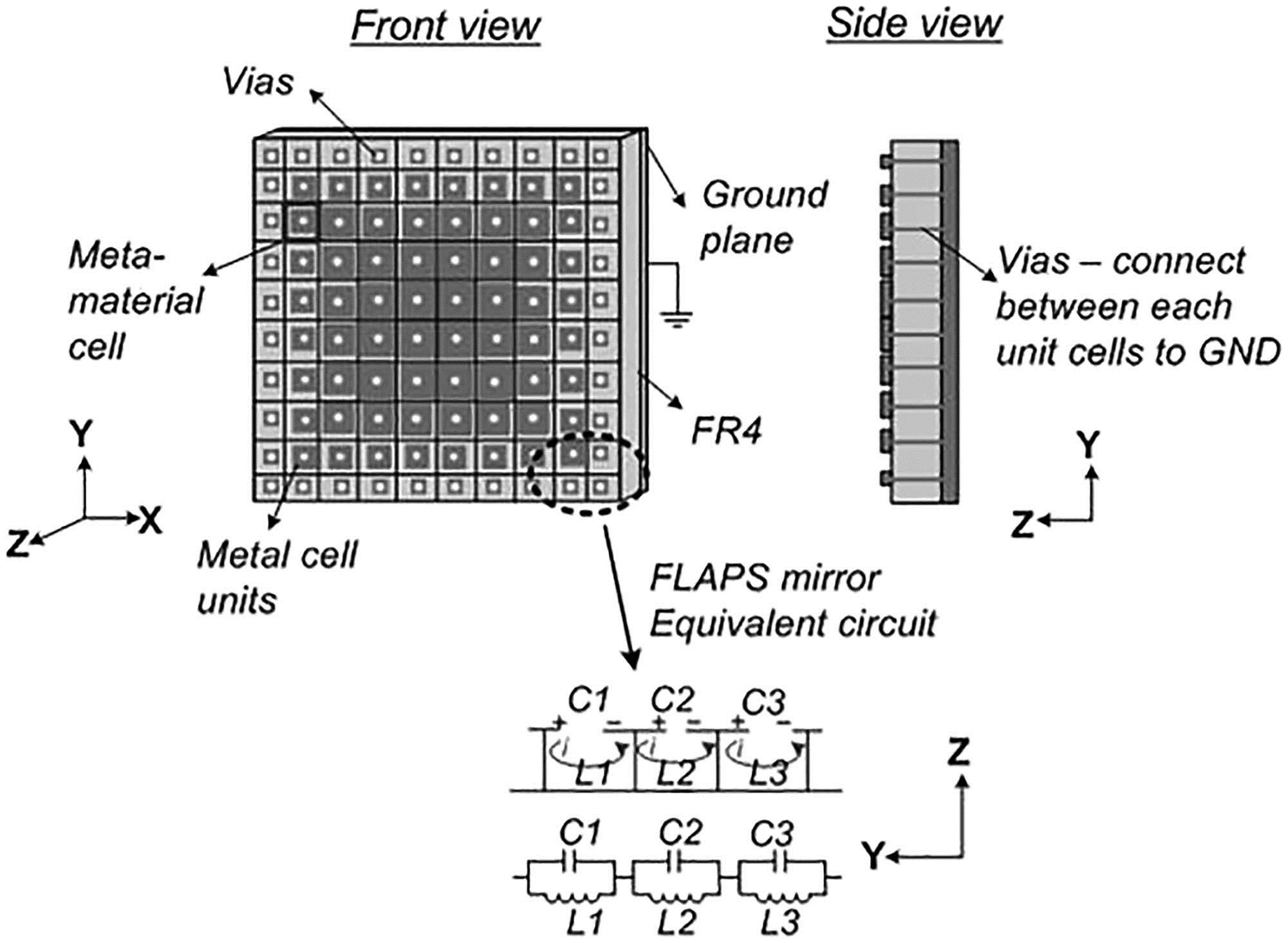
    Fig. 1. Proposed reflector structure composed of an FR4 (glass epoxy) dielectric substrate with a ground plane on the back and printed metal patterns on the front. Each metal cell on the front is connected to the back ground plane by a via. The metal cells in the center are the largest, and they gradually decrease in size as they approach the edges of the FLAPS mirror. The FLAPS mirror cells can be described as an array of parallel LC resonance circuits.
    Top: Side view of parabolic mirror and parallel rays L1, L2, and L3 reflected to focal point F due to the mirror geometry. Bottom: Side view of FLAPS structure and parallel rays L1, L2, and L3 reflected to the same focal point F due to the phase shift provided by each cell of the FLAPS.
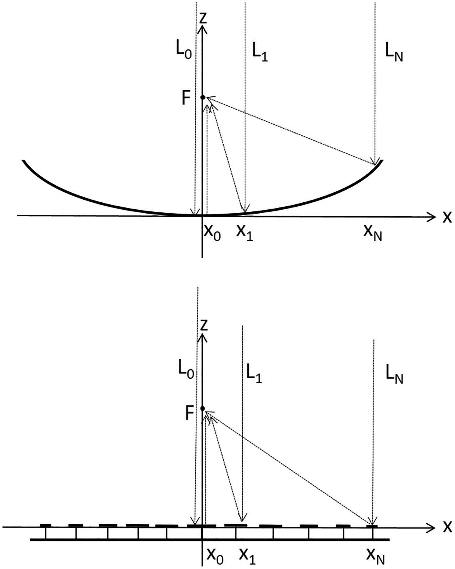
    Fig. 2. Top: Side view of parabolic mirror and parallel rays L1, L2, and L3 reflected to focal point F due to the mirror geometry. Bottom: Side view of FLAPS structure and parallel rays L1, L2, and L3 reflected to the same focal point F due to the phase shift provided by each cell of the FLAPS.
    Simulation model. a. Top surface dimensions gradually increase after every simulation session. b. The region between the top plane and the port is filled by a vacuum.
    Fig. 3. Simulation model. a. Top surface dimensions gradually increase after every simulation session. b. The region between the top plane and the port is filled by a vacuum.
    Top: Simulation results for S11 phase shift. Bottom: Simulation results for S11 magnitude. Each curve represents a different patch size. 1: 0.57 mm, 2: 0.54 mm, 3: 0.51 mm, 4: 0.48 mm, 5: 0.54 mm, 6: 0.42 mm, 7: 0.39 mm, 8: 0.36 mm, 9: 0.33 mm, and 10: 0.30 mm. When the size of the PEC on the top surface of the FLAPS mirror is gradually decreased, the phase curve moves to the right on the frequency axis and vice versa.
    Fig. 4. Top: Simulation results for S11 phase shift. Bottom: Simulation results for S11 magnitude. Each curve represents a different patch size. 1: 0.57 mm, 2: 0.54 mm, 3: 0.51 mm, 4: 0.48 mm, 5: 0.54 mm, 6: 0.42 mm, 7: 0.39 mm, 8: 0.36 mm, 9: 0.33 mm, and 10: 0.30 mm. When the size of the PEC on the top surface of the FLAPS mirror is gradually decreased, the phase curve moves to the right on the frequency axis and vice versa.
    Experimental setup. Instead of one of the parabolic mirrors, the FLAPS mirror was tilted 20° relative to the optical axis to avoid optical aberrations, and in front of it, a track with a TK sensor was placed and replaced later by a Spiricon camera.
    Fig. 5. Experimental setup. Instead of one of the parabolic mirrors, the FLAPS mirror was tilted 20° relative to the optical axis to avoid optical aberrations, and in front of it, a track with a TK sensor was placed and replaced later by a Spiricon camera.
    Maximum response of the TK sensor for 94, 97, and 100 GHz was obtained for a distance of 65 cm from the FLAPS mirror.
    Fig. 6. Maximum response of the TK sensor for 94, 97, and 100 GHz was obtained for a distance of 65 cm from the FLAPS mirror.
    Energy scattering as observed on the Spiricon camera when it is located at the focal point of the FLAPS mirror. The bright color in the center is an indication of the maximum density spot, and the energy density becomes lower as the outer rings are approached. The photo size is 12 mm×12 mm, and the size of the MMW beam spot is about 5 mm×6 mm.
    Fig. 7. Energy scattering as observed on the Spiricon camera when it is located at the focal point of the FLAPS mirror. The bright color in the center is an indication of the maximum density spot, and the energy density becomes lower as the outer rings are approached. The photo size is 12mm×12mm, and the size of the MMW beam spot is about 5mm×6mm.
    Gil Litmanovitch, David Rrotshild, Amir Abramovich. Flat mirror for millimeter-wave and terahertz imaging systems using an inexpensive metasurface[J]. Chinese Optics Letters, 2017, 15(1): 011101
    Download Citation