Gil Litmanovitch, David Rrotshild, Amir Abramovich. Flat mirror for millimeter-wave and terahertz imaging systems using an inexpensive metasurface[J]. Chinese Optics Letters, 2017, 15(1): 011101
Copy Citation Text
Flat mirrors, also known as flat parabolic surfaces, for millimeter-wave and terahertz imaging systems are demonstrated. This flat mirror is based on the metasurface in which an inexpensive printed circuit board technology is used to realize copper patterns printed on an FR4 substrate. Compared to the conventional reflector antennas used today in diverse applications (for homeland security, medical systems, communication, etc.), the suggested mirror has major advantages in process simplicity, mechanical flexibility, frequency alignment, weight, and cost. The theoretical background, simulation results, experimental results, and proof of concept are given in this Letter.
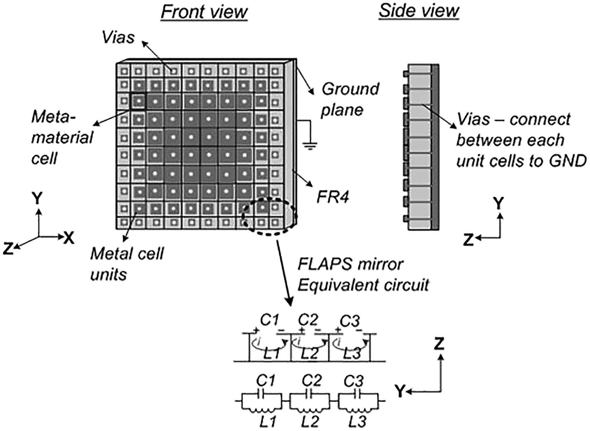
In recent years, the use of millimeter-wave (MMW) applications (for homeland security, communication, medicine, etc.) has grown significantly, especially in the case of applications based on imaging systems[1]. The lack of quasi-optical components for the 30–300 GHz frequency range, such as large-aperture mirrors and inexpensive detectors and sources, is noticeable. The high cost, complicated production processes, and alignment difficulties call for the development of low-cost MMW components for quasi-optical and imaging systems[2]. A good example of such a component is the glow discharge detector, which is a very inexpensive detector for MMW imaging systems that costs about $0.30[3–5]. On the other hand, the imaging mirror is very expensive and very difficult to align due to its weight and large aperture. Mirrors with large apertures equal to 500 mm and greater are required for proper MMW image quality and maintenance of the focal point generally close to its diffraction limit[6]. In this Letter, we will present an alternative imaging mirror design based on a planar surface for MMW imaging, which is very inexpensive and lightweight and is known as a flat parabolic surface (FLAPS)[7]. This FLAPS design is based on an array of variable-dimension metal cells (a metasurface), which are connected to the ground plane through a dielectric substrate. This unique structure is a particular case of two-dimensional (2D) metamaterial called a metasurface[8]. The dielectric constants of the substrate and size of each metal cell determine its electrical characteristics, such as capacitance and inductance, as well as its electromagnetic properties[9]. MMW radiation incident to the FLAPS mirror surface causes currents to flow from the top surface of the dipoles to the ground plane through a passive array of capacitors and inductors, which cause a phase shift in the reflected electromagnetic wave (see Fig. 1). By varying the size of a dipole, we basically vary its phase shift, depending on its location on the FLAPS mirror surface (see Fig. 1). In this study, the metasurface mirror structure was composed of an FR4 (glass epoxy) dielectric substrate with a ground plane in the back and printed metal patterns on the front. Each metal cell on the front is connected to the back ground plane by a via, which is coated by a micron layer of copper to enable electrical conductivity from the metal cell to the ground plane (see Fig. 1). Unlike a unified ground plane, the dimensions of the metal cells on the front are variable. The metal cells in the center are the largest, and they gradually decrease in size as they approach the edges of the FLAPS (metasurface) mirror.
Figure 1.Proposed reflector structure composed of an FR4 (glass epoxy) dielectric substrate with a ground plane on the back and printed metal patterns on the front. Each metal cell on the front is connected to the back ground plane by a via. The metal cells in the center are the largest, and they gradually decrease in size as they approach the edges of the FLAPS mirror. The FLAPS mirror cells can be described as an array of parallel LC resonance circuits.
The FLAPS mirror cells can be described as an array of parallel LC resonance circuits (illustrated in Fig. 1)[9]. The capacitance is created due to the dielectric gap between two adjacent metal pads, and the inductance is created due to the current path through the metal pads and the via. The value of the capacitance is determined by the dimensions of the copper pad (), the FR4 thickness (), the gap between adjacent pads (), the vacuum permittivity (), and the permittivity of FR4 ( at 100 GHz). The inductance value, however, is determined by the permeability constant (, ) and the dielectric thickness. The relations for the capacitance and inductance are given by
The variation of the size of the copper pads (see Fig. 2) as a function of their location on the FLAPS alters the values of and ; therefore, it alters the cell’s resonance frequency (), the surface impedance, and the reflected phase shift accordingly. Expressions for the impedance () and resonance frequency () of each cell are given by[10]
Sign up for Chinese Optics Letters TOC. Get the latest issue of Chinese Optics Letters delivered right to you!Sign up now
Figure 2.Top: Side view of parabolic mirror and parallel rays , , and reflected to focal point due to the mirror geometry. Bottom: Side view of FLAPS structure and parallel rays , , and reflected to the same focal point due to the phase shift provided by each cell of the FLAPS.
From Eqs. (3) and (4), we can learn that the lower the frequency is, the more dominant the inductive reactance becomes, and the higher the frequency is, the more dominant the capacitive reactance becomes. Near the resonance frequency (), however, the surface impedance is very high. Electromagnetic waves impinging on the FLAPS mirror sense different impedance and experience a different phase shift, depending on the , coordinates on the FLAPS metasurface[10]. With the proper design of the geometry of the cell array, a wide, collimated MMW beam is reflected, causing the convergence of the spherical wave into a single focal point. In common reflectors with a low-impedance surface, surface waves propagate along the surface until they reach its interface with free space at an edge or a corner. Furthermore, if an array of reflectors sharing the same ground plane is used, it may cause mutual magnetic and electric coupling between adjacent reflectors, which can reduce the reflector radiation qualities and cause the appearance of ripples in the radiation signal pattern[11]. The proposed FLAPS mirror structure generates a network of parallel LC resonance circuits (see Fig. 1), which have a high-impedance surface within the resonance frequency () band and thereby suppress the surface waves propagating over the surface[12]. When this phenomenon was analyzed for E-plane and H-plane coupling, it was discovered that both are reduced as the dielectric substrate of the reflector becomes thinner. However, the dielectric constant influences the E-plane and H-plane coupling differently. When the dielectric constant is high, propagation along the E-plane direction is dominant; therefore, the mutual coupling in the E-plane will be stronger and the H-plane coupling will be weaker under those conditions. By properly designing the array of metal cells on the FLAPS mirror surface, we will create a high-impedance surface, and surface waves will be suppressed. The electromagnetic bandgap of the suppressed frequency will be determined by the LC resonance frequency (). The average energy on the surface will be reduced proportionally to the ground surface area (), as indicated by[12]
The design of the FLAPS mirror was based on a 2D parabolic function, as can be seen at the top of Fig. 2.
In order to realize a focal point at , the parabolic function should be in the form shown in Eq. 6, and thus, is given by Eq. 7,
Calculations of the required phased shift of each patch in the metasurface cell along the - and -axes are based on the phased array theory[13]. Each patch in the designed FLAPS will be denoted by its position (see the bottom of Fig. 2), where , are array indices and the array size is , where is an even integer. The optical path difference between two adjacent cells to the focal point is described by and the phase shift between two adjacent cells would be If we compensate and add phase value to each unit cell relative to , where the reflected phase of is the reference phase, a parabolic reflector can be implemented. The same calculations hold for the -axis of the FLAPS. For cells that are not on the - and -axes, Eq. (8) is only an approximation.
According to the FLAPS mirror and the LC circuit model shown in Fig. 1, the FLAPS metasurface mirror designed for MMW imaging systems is composed of two metal layers with a dielectric substrate (FR4) between them. The bottom layer is a unified copper plane (0.035 mm thick), which serves as the ground plane. The top layer contains square cells designed to shift the reflected phase of the incident wave. A single cell is (about 1/3 of the wavelength for 100 GHz). Each cell has a square copper pad with similar geometry, but it varies along the surface (the thickness of each copper pad is 0.035 mm). The pad size in each cell varies as the edges of the FLAPS are approached from a maximum of in the center to at its edges. There are 60 pad frames in this FLAPS mirror, and they decrease in 20 μm steps per pad as the FLAPS metasurface edge is approached. The substrate material used is well-known FR4, whose dielectric permittivity is at 100 GHz, and the thickness is 0.1 mm. A via in the center of each cell is used to connect the metal pads located on the top surface of the FLAPS to the ground plane. The diameter of each via is 150 μm, and each via is coated with a few microns of copper to enable electrical conductivity between the metal pads and ground plane. The distance between two adjacent vias in the FLAPS mirror is 1 mm in all directions. The physical dimensions of the FLAPS mirror are , and it is made of 60 frames of metal pads (the total number of pads is 14,400).
Simulations of the FLAPS designed were carried out using a computer simulation technology (CST) transient solver. We designed a metal cell that represents a single cell from the array on our FLAPS mirror surface. The cell consists of square metal planes on its top and bottom separated by a dielectric substrate (FR4). For the top and bottom metal planes, we used perfect electromagnetic conductors (PECs), which were connected by top-to-bottom vias (150 μm in diameter). Figure 3(a) shows models of single cells in three different locations on the FLAPS. Port 1 of the CST device is located 10 mm from the reflector’s front surface (-axis) in order to simulate the S11 phase shift, as shown in Fig. 3(b). During the simulation, the size of the front patch was varied from to in steps.
Figure 3.Simulation model. a. Top surface dimensions gradually increase after every simulation session. b. The region between the top plane and the port is filled by a vacuum.
Figure 4 shows simulation results of the S11 phase shift as a function of the frequency for cells with different sizes of the top metal surfaces, which vary gradually from to . By selecting 100 GHz, for example, a FLAPS mirror that will behave as a parabolic front-wave reflector that will focus an incident plane wave into a focal point can be designed (see Fig. 1).
Figure 4.Top: Simulation results for S11 phase shift. Bottom: Simulation results for S11 magnitude. Each curve represents a different patch size. 1: 0.57 mm, 2: 0.54 mm, 3: 0.51 mm, 4: 0.48 mm, 5: 0.54 mm, 6: 0.42 mm, 7: 0.39 mm, 8: 0.36 mm, 9: 0.33 mm, and 10: 0.30 mm. When the size of the PEC on the top surface of the FLAPS mirror is gradually decreased, the phase curve moves to the right on the frequency axis and vice versa.
According to the simulation results shown in the bottom of Fig. 4, the maximum difference in magnitudes around 100 GHz is about 8%, so for our calculations, it can be assumed that the reflected intensity for all patch sizes is the same. Note that we used the transient solver of the CST. The transient solver uses a pulse in time, which is non-stationary signal. Thus, the simulated model [see Fig 3(b)] can “store” energy and can be obtained.
A FLAPS mirror was fabricated using an FR4 substrate and a standard PCB production process according to the simulation results in Fig. 4 and the structure shown in Fig. 1. Allegro software was used to prepare the FLAPS production files. The overall dimensions of the FLAPS reflector were (including the margins for the mechanical holder). Electromagnetic performance experiments were carried out on the FLAPS by a high-resolution spectroscopic system operating in the W band at 92–100 GHz[14,15]. The experimental setup (see Fig. 5) contains a tunable W-band radiation source based on a frequency multiplier from Virginia Diodes Inc., which provides high CW power up to 250 mW[14]. The W-band radiation is coupled out to free space using a standard, linearly polarized pyramidal horn antenna. An MMW camera (Spiricon Inc.) is located in the focal plane of the FLAPS mirror. The Spiricon MMW camera has a focal plane array made of a pyroelectric crystal measuring .
Figure 5.Experimental setup. Instead of one of the parabolic mirrors, the FLAPS mirror was tilted 20° relative to the optical axis to avoid optical aberrations, and in front of it, a track with a TK sensor was placed and replaced later by a Spiricon camera.
At first, a sensitive MMW detector (from Thomas Keating Inc., TK) was used to find the location of the focal plane of the FLAPS. The TK device is a photo-acoustic detector, which creates a voltage proportional to the incident electromagnetic wave. The energy from the horn antenna was collimated into the FLAPS mirror using an off-axis parabolic mirror with a diameter of 76.2 mm and a focal length of 127 mm. The TK detector was inserted instead of the camera, as illustrated in Fig. 5, in order to align and optimize the system’s performance. The FLAPS mirror was rotated 20° relative to the optical axis. Larger rotations may increase the optical aberrations. The performance of the FLAPS mirror was tested at three frequencies: 94, 97, and 100 GHz. Figure 6 shows the power measured at the three frequencies as a function of the distance between the FLAPS mirror and the sensor.
Figure 6.Maximum response of the TK sensor for 94, 97, and 100 GHz was obtained for a distance of 65 cm from the FLAPS mirror.
The experimental results show that the maximum power was obtained when the TK sensor was located 65 cm from the reflector. This indicates that the focal length of the FLAPS mirror fabricated is approximately 65 cm, which is in excellent agreement with the phase shift model derivation [see Eqs. (6)–(9)]. Additional information that can be obtained indicates the FLAPS is a frequency-selective surface, as expected. A higher response was measured at 100 GHz than at 97 and 94 GHz (46, 20, and 7 mV, respectively).
Figure 7 shows the power pattern as captured by the Spiricon camera when located at the focal point of the FLAPS mirror (65 cm from the FLAPS). The scale on the right-hand side indicates the relative power level on the Spiricon camera detector. The bright color in the center is an indication of the maximum density, and the power density becomes lower as the outer rings are approached. The size of the beam spot size is about , which is close to the diffraction limit[6]. An analysis of the results from the camera reveals that the FLAPS mirror focuses incident MMW electromagnetic rays into a single focal point, confirming the results in Fig. 6.
Figure 7.Energy scattering as observed on the Spiricon camera when it is located at the focal point of the FLAPS mirror. The bright color in the center is an indication of the maximum density spot, and the energy density becomes lower as the outer rings are approached. The photo size is , and the size of the MMW beam spot is about .
The results presented in this Letter are in good agreement with the theory, simulation results, and mathematical calculations. Each metal cell on the FLAPS designed has electromagnetic properties that depend on its dimensions, as shown in Fig. 4. By properly designing the resonance frequency, the propagation in the H-plane and the E-plane is decreased, enabling the development of the FLAPS. The FLAPS is fabricated using inexpensive well-known FR4 technology. The FLAPS designs exhibits a focusing performance close to the diffraction limitx]6] (see Fig. 7). Reflectors of this kind can be used in MMW imaging systems, medical applications, homeland security, communication, military applications, etc. We strongly believe that this study can serve as a foundation for future MMW imaging systems and provide simplicity of design and fabrication, as well as low cost. Furthermore, the need to employ the MMW band in the fifth generation of mobile communication in order to increase the data rate requires such FLAPS to direct and focus the MMW radiation on the user.
References
[1] D. Liu, B. Gaucher, U. Pfeiffer, J. Grzyb. Advanced Millimeter-Wave Technologies: Antennas, Packaging and Circuits(2009).
[2] L. J. Sikora. ‘Commercial Applications and Dual-Use Technology,’ Conference Proceedings, 233(1993).
[13] M. W. Niaz, Z. Ahmed, M. B. Ihsan. German Microwave Conference Digest of Papers(2010).
[14] E. Gross, A. Abramovich, C. Bruma, E. Farber. COMCAS IEEE International Conference on Microwaves, Communications, Antennas and Electronics Systems, 1(2009).
[15] O. Malca, E. Danieli, S. Gabay, A. Zilberman, N. S. Kopeika, A. Schechter, A. Abramovich. Microwaves, Communications, Antennas and Electronics Systems(2011).
Gil Litmanovitch, David Rrotshild, Amir Abramovich. Flat mirror for millimeter-wave and terahertz imaging systems using an inexpensive metasurface[J]. Chinese Optics Letters, 2017, 15(1): 011101