Abstract
We experimentally demonstrate a 16 × 16 reconfigurably nonblocking optical switch fabric using a Benes architecture. The switch fabric consists of 56 2 × 2 Mach–Zehnder interferometer based elementary switches, with each integrated with a pair of waveguide microheaters. The average on-chip insertion loss is ~5.2 dB for both of the “all-cross” and the “all-bar” states, with a loss variation of 1 dB over all routing paths. The cross talk for all switching states is better than ?30 dB. The switching time of the switch element is about 22 μs. The switching functionality is verified by transmission of a 40 Gb∕s quadrature phase-shift keying optical signal.1. INTRODUCTION
According to the forecast of Cisco, the annual Internet Protocol (IP) traffic will surpass the 2 zettabyte threshold in 2019, and the IP traffic will grow at a compound annual growth rate of 23% from 2014 to 2019 [1]. The continuous demand for higher data transmission bandwidth requires energy-efficient switching to support the ever-growing intelligent and programmable optical networks. A hybrid network architecture will be envisioned in the future to take advantage of both electrical and optical switching [2]. The electrical switching can be used for small bursty data flows and data processing intensive applications while the optical switching is suitable for larger data flow traffic. Optical switches have the advantages of high switching capacity, low power consumption, and compact size compared with their electrical counterparts. Over the past years, a variety of optical switch technologies have been developed based on micro-electromechanical system (MEMS) actuators [3,4], silica-based planar lightwave circuits (PLCs) [5,6], and III–V materials [7,8]. Silicon photonics has been regarded as one of the most promising technologies for the merits of monolithic integration with microelectronic drive circuits and potentially low-cost, large-volume production.
Many thermo-optic (TO) [9–14] and electro-optic (EO) [15–21] switches have been reported in recent years. EO switches possess fast switching time (a few nanoseconds) but have high cross talk and insertion loss due to the electro-absorption effect associated with the electrorefraction effect after free-carrier injection. On the contrary, the TO switches remain low loss, but the switching time is intrinsically limited to microseconds. In the hybrid network systems, the optical switches are used to process the slow but large-flow optical traffic, and therefore the TO switches are preferred for their low loss and low cross talk. A TO switch has been demonstrated [10]. It has a narrow transmission bandwidth of 1.8 nm for cross talk below , and the on-chip insertion loss is 15.8 dB.
In our previous work, we have experimentally demonstrated two types of TO switches based on cascaded multimode interferometers (MMIs) [12,13]. The cross talk is relatively high due to the imperfect power splitting of MMIs. In this paper, we present a reconfigurably nonblocking silicon TO switch based on Mach–Zehnder interferometers (MZIs) actuated with waveguide microheaters. The chip has a footprint of . The average on-chip insertion loss of the switch is about 5.2 dB, and the cross talk is below in a bandwidth of 10 nm for all states. Optical transmission of a 40-Gb/s quadrature phase-shift keying (QPSK) signal verifies the fidelity of the signal after passing through the switch chip.
Sign up for Photonics Research TOC. Get the latest issue of Photonics Research delivered right to you!Sign up now
2. DEVICE DESIGN AND FABRICATION
The switch is constructed based on a Benes structure, as shown in Fig. 1. The Benes architecture is reconfigurably nonblocking and requires the minimum number of switching elements to obtain the complete switch states. It possesses the lowest insertion loss compared to crossbar, switch-and-select, path-independent insertion-loss (PILOSS), N-stage planar, and other architectures. A Benes architecture comprises switch elements. Each routing path goes through seven stages of switch elements. As each element has two states, the switch hence has states in total, among which 16! states are necessary for the complete mapping. The inset shows the structure of the switch element. It is composed of two MMIs with waveguide microheaters integrated in both arms for TO tuning of the silicon refractive index. The design of the microheater can be found in [17]. The microheater is designed to be 400 μm long in order to achieve a phase shift at a low drive voltage. It is surrounded by air trenches to prevent heat lateral diffusion. The ridge waveguide has a high resistivity working as a microheater, so heat is generated inside the waveguide and directly interacts with the optical mode. Compared with other metallic heaters, our design based on the waveguide heater has higher tuning efficiency and faster temporal response [22]. There are multiple waveguide crossings in the Benes architecture, leading to extra insertion loss and cross talk. We employ MMI based on the self-imaging effect at the crossing to reduce the insertion loss and cross talk. The detailed designs and experimental results of the MMIs and waveguide crossings can be found in [19].
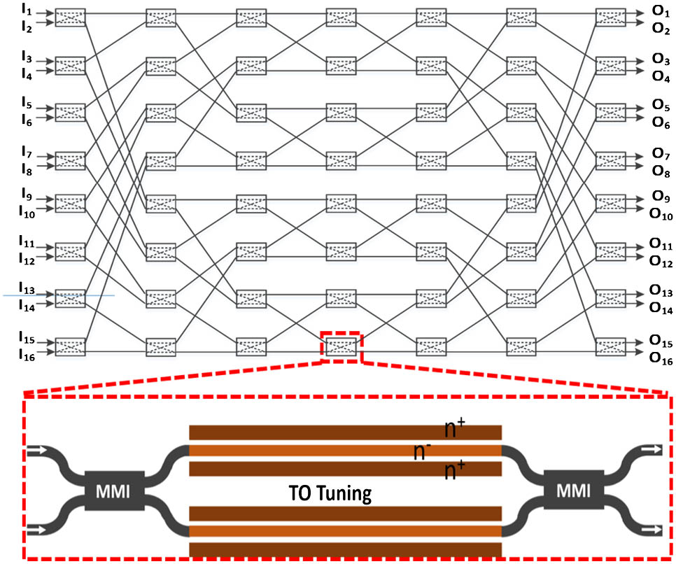
Figure 1.Schematic of the optical switch. Inset shows the structure of the MZI switch element.
The chip was fabricated on a silicon-on-insulator (SOI) wafer using the complementary metal-oxide semiconductor (CMOS)–compatible process in IME Singapore. Figure 2(a) shows the microscope image of the fabricated devices. The chip size is . The inset illustrates the magnified MZI switch elements. All input and output waveguides are terminated with grating couplers and positioned in the chip center to couple with a fiber array. The electrical pads are put close to the chip edges to favor wire-bonding with a printed circuit board. A 32-channel 127-μm-pitch fiber array is attached to the switch chip by using ultraviolet (UV) light curable adhesive, whose refractive index is close to that of silicon dioxide. The coupling loss after the optical package is about . Figure 2(a) shows a microscope image of the switch. Figures 2(b) and 2(c) show the photos of the packaged switch chip.

Figure 2.(a) Optical microscope image of the switch chip. The inset shows the zoomed-in view of the MZI switch elements. (b) Photo of the switch in a sealed metal box. (c) Photo of the switch after electrical and optical package. The inset shows the zoomed-in view of a fiber array attached to the switch chip using UV-curable adhesive.
3. EXPERIMENTAL RESULT
A. Switch Element Characterization
We first measured the performance of the individual MZI switch element. Figure 3 shows the transverse electric (TE) polarization transmission spectra of the “cross” and “bar” states upon TO tuning. The spectra are normalized to a test waveguide to eliminate the impact of grating couplers. As there exist phase errors in the MZI arms induced by imperfect fabrication, an initial bias ( power) is required to reach the complete cross state. The TO power consumption to change the switch from the cross state to the bar state is . The insertion loss for the individual switch element is about 0.32 dB. The minimum cross talk at 1560 nm wavelength is less than for both states. The switch element has a bandwidth of about 30 nm, in which the cross talk is less than . The low cross talk and high switching extinction ratio suggest that the MMIs have an even splitting ratio.
Figure 3.Transmission spectra at different TO power consumptions for the cross port and the bar port of an MZI switch element.
B. Insertion Loss of the 16×16 Switch
We tuned all 56 MZI switch elements to the cross state by applying proper voltages to the microheaters to correct phase errors. In this case, the switch chip was at the all-cross state. Then all switch elements were changed from the cross to the bar state by introducing a phase shift in one of the MZI arms in each element. The switch was hence configured to the all-bar state. Figure 4 shows the TE transmission spectra for all routing paths at the all-cross and the all-bar states. The average on-chip insertion loss at both states is at 1560 nm, with a variation of 1 dB over all optical paths. The loss variation mainly comes from the difference in the waveguide length and the number of waveguide crossings along an optical path. The on-chip insertion loss is contributed by three parts: switch element loss, waveguide crossing loss, and waveguide loss. Each switch element has a loss of 0.32 dB, and therefore the aggregated loss of seven switch elements in an optical path is 2.24 dB. One waveguide crossing has an insertion loss of 0.05 dB measured from a test structure, and thus the loss caused by waveguide crossings (11 crossings on average) is 0.55 dB. The waveguide loss is hence estimated to be 2.41 dB. As the waveguide length from an input to an output port is around 2 cm, the waveguide propagation loss is around . The relatively low waveguide loss results because 2-μm-wide waveguides are used for long connections between switch elements.
Figure 4.Transmission spectra of all optical paths at the all-cross and the all-bar states of the switch.
C. Cross Talk of the 16×16 Switch
Figures 5 and 6 show the full set of TE transmission spectra of the optical switch at the all-cross and the all-bar states, respectively. Each plot groups 16 spectra from all 16 input ports to one output port. We can see that the cross talk of the switch is lower than over a 10-nm bandwidth centered at 1560 nm for both states. The cross talk is mainly generated from the switch elements, being the primary source for signal degradation after switching. Each optical path passes through seven switching elements, and cross talk will be added in from other optical paths at each intersecting element due to the limited switching extinction ratio. There are three cases in terms of the intersection scenarios of two optical paths: no intersection, single intersection, and two intersections. If the two optical paths do not intersect, there is no direct interaction between them and the cross talk is very low. A single intersection will cause certain cross talk to either of the two paths. The worst case is when the two optical paths intersect twice, which inevitably leads to interference, and the cross talk rises at certain wavelengths. This is also the reason why we observe periodic fluctuations in some of the cross-talk spectra in Figs. 5 and 6. Besides these two special switching states, our switch fabric can also be conveniently configured to any of the 16! states necessary for nonblocking operation.
Figure 5.Measured transmission spectra of the switch at the all-cross state.
Figure 6.Measured transmission spectra of the switch at the all-bar state.
D. Switching Power and Speed
The power consumption of all the 56 switch elements at the all-cross and the all-bar states is listed in Table 1. It should be noted that due to the presence of random fabrication errors, the phase correction power to reach the cross state also varies randomly.
| | S1(mW) | S2(mW) | S3(mW) | S4(mW) | S5(mW) | S6(mW) | S7(mW) |
| | all “0” | all “1” | all “0” | all “1” | all “0” | all “1” | all “0” | all “1” | all “0” | all “1” | all “0” | all “1” | all “0” | all “1” |
| 1 | 3.86 | 28.0 | 24.5 | 48.7 | 40.7 | 10.7 | 9.83 | 26.3 | 3.63 | 19.6 | 5.10 | 24.6 | 3.27 | 23.6 |
| 2 | 4.20 | 25.6 | 3.18 | 24.2 | 10.0 | 27.1 | 0.85 | 20.1 | 1.30 | 18.6 | 1.66 | 21 | 24.7 | 45.5 |
| 3 | 3.26 | 25.3 | 1.78 | 20.4 | 1.90 | 20.4 | 7.95 | 27.6 | 13.9 | 34.2 | 14.3 | 33.7 | 5.73 | 23.7 |
| 4 | 7.97 | 28.5 | 5.70 | 26.6 | 6.26 | 24.1 | 2.42 | 19.9 | 0.44 | 18.8 | 3.49 | 24.7 | 3.64 | 22.6 |
| 5 | 12.2 | 36.0 | 4.94 | 24.0 | 9.06 | 29.4 | 7.42 | 28.4 | 3.34 | 22.7 | 10.2 | 29.3 | 40.3 | 11.4 |
| 6 | 4.49 | 24.6 | 2.05 | 19.8 | 4.88 | 26.0 | 9.73 | 30.9 | 6.44 | 26.9 | 13.8 | 32.5 | 1.85 | 20.4 |
| 7 | 20.5 | 42.3 | 32.4 | 6.40 | 1.42 | 21.2 | 3.55 | 22.7 | 3.35 | 21.2 | 9.56 | 28.3 | 1.22 | 18.1 |
| 8 | 1.58 | 21.7 | 17.4 | 35.9 | 27.0 | 3.64 | 8.69 | 28.6 | 19.6 | 39.7 | 6.26 | 24.7 | 15.4 | 34.6 |
Table 1. Power Consumption at the All-Cross and the All-Bar Statesa
The total power consumption is 515 mW at the all-cross state and 1428 mW at the all-bar state. It should be noted that, in the above measurement, the TO tuning was performed to one fixed arm of the MZI element at both states. The power could be reduced if TO tuning is performed on both arms.
We also characterized the switching speed of the device by measuring the switch element’s time-domain response. A 500 Hz electrical square-wave signal is applied to one waveguide microheater via a radio frequency (RF) probe. The peak-to-peak drive voltage is with a DC bias voltage of . The output modulated optical signal is measured as shown in Fig. 7. The rise/fall time of the switch element is .
Figure 7.Time-domain optical response of the switch element. (a) Applied square-wave electrical drive signal. (b) Measured optical waveform. The dashed lines indicate the 10% and 90% power levels.
E. QPSK Signal Switching
In order to verify the switching capability for high-speed optical signals, we performed system transmission experiments using QPSK optical signals. The QPSK signal was generated by modulating a continuous wave (CW) light at 1560 nm wavelength using a based in-phase/quadrature vector modulator. The modulator was driven by two eudorandom bit sequence RF signals from two pulse-pattern generators, so the optical signal bit rate was . The optical signal was then amplified by an erbium-doped fiber amplifier (EDFA) followed by a polarization controller to set the TE polarization before it was coupled into the chip by grating couplers. In order to compensate the loss of the device, the output optical signal was amplified by another EDFA, followed by a bandpass filter to suppress the amplified spontaneous emission noise from the EDFAs. A variable optical attenuator was used to adjust the optical power before the optical signal was received and analyzed by an optical modulation analyzer (Agilent, N4392A). The error-vector magnitude (EVM) was obtained from the measured constellation diagrams.
We measured the optical signal transmission for the all-cross and the all-bar states. The QPSK signal was injected into only one port at a time. Figure 8(a) shows the constellation diagram of the system back-to-back (BtB) transmission, with an EVM of 8.09%. Figures 8(b) and 8(c) depict the constellation diagrams of all the 16 light paths at the all-cross and the all-bar states, respectively. The measured EVMs are all smaller than 9.24%, indicating the signal is degraded by less than 1.15% after passing through the chip. It demonstrates that our switch is capable of switching QPSK signal with a high signal quality.
Figure 8.Measured constellation diagrams of a QPSK signal. (a) BtB transmission, (b) the all cross state, and (c) the all bar state.
4. DISCUSSION
Table 2 summarizes the key performance of the state-the-art high-port-count silicon optical switch fabrics. Compared with other reported silicon switch fabrics, our TO switch has an overall balanced superior performance in terms of insertion loss, cross talk, and response speed. The EO switches based on possess the merit of a short switching time of a few nanoseconds, but they also have a higher insertion loss and a worse cross talk due to the free carrier absorption effect. The reported highest-port-count silicon EO optical switches are the switches [19], in which the worst cross talk is around . Compared with other metallic heaters (e.g., TiN), our waveguide heater has higher tuning efficiency and faster temporal response. The power consumption to change the switch state using a typical TiN heater with air trenches is around 35 mW, larger than the waveguide-type heater. The power consumption can be further reduced by etching off the silicon substrate. Conventional MEMS mirror-based switches have many disadvantages in terms of switching time, stability, and chip size. The recently reported MEMS-actuated optical switch combines the merits of silicon PLCs and MEMS actuation, in which low insertion loss and fast switching time have been achieved [3], but a high drive voltage of 42 V is required in order to actuate the MEMS cantilevers. This high drive voltage inhibits its integration with microelectronic chips. Its sensitivity to environmental vibration also remains as a potential issue for long-term stable operation.
| Technologies | Port Count | Topology | Insertion Loss (dB) | Cross Talk (dB) | Power Consump. (mW) | Reconfig. Time (μs) | Footprint (mm2) |
| [20] (MZI, TiN+p−i−n) | 8×8 | Blocking | NA | −15 to −5 (20 nm) | 4.4–32.2 | 0.012 | NA |
| [14] (MZI, TiN) | 8×8 | Switch and Select | 4±0.8 | −45 (30 nm) | 70 | 250 | 8×8 |
| [11] (MZI, TiN) | 8×8 | PILOSS | 6.5±1 | −23.1 | NA | NA | 3.5×2.4 |
| [19] (MZI, TiN+p-i-n) | 16×16 | Benes | 6.7−13.9±1 | −20 to −10 (30 nm) | 881+289 | 0.006 | 10.7×4.4 |
| [10] (MZI, TiN) | 32×32 | PILOSS | 15.8±1 | −20 (1.8 nm) | 2930 | 30 | 11×25 |
| [4] (MEMS-actuation) | 50×50 | Cross-bar | <27.5 | <−20 (13 nm) | NA | 3.8 | 9×9 |
| [3] (MEMS-actuation) | 64×64 | Cross-bar | <3.7 | −20 | NA | 0.9 | 8.6×8.6 |
| This work (MZI, WG heater) | 16×16 | Benes | 5.2±1 | ∼−30 (10 nm) | 515+913 | 21.78 | 7×3.6 |
Table 2. Performance Comparison of Reported High-Port-Count Silicon Switch Fabrics
5. CONCLUSIONS
We have designed and experimentally demonstrated a compact, low loss, and low cross talk reconfigurably nonblocking optical switch. The switch chip is based on a Benes structure and consists of MZIs, with each arm integrated with a waveguide microheater. The switch chip is built on the SOI platform using the CMOS-compatible process with a footprint of only . The on-chip insertion loss is 5.2 dB at 1560 nm, and the worst cross talk is better than over a 10-nm bandwidth. The switching power for each switch element to change the state is about 22 mW. The power consumption could be reduced if TO tuning is performed on both arms. The switching time is around 22 μs. Optical signal transmission experiments using a QPSK signal confirm the signal fidelity after passing through the switch chip.
Acknowledgment
Acknowledgment. We acknowledge IME Singapore for device fabrication.
References
[1] C. V. N. Index. Forecast and Methodology, 2014–2019(2015).
[2] D. Kilper, K. Bergman, V. W. Chan, I. Monga, G. Porter, K. Rauschenbach. Optical networks come of age. Opt. Photon. News, 25, 50-57(2014).
[3] T. J. Seok, N. Quack, S. Han, R. S. Muller, M. C. Wu. Large-scale broadband digital silicon photonic switches with vertical adiabatic couplers. Optica, 3, 64-70(2016).
[4] S. Han, T. J. Seok, N. Quack, B.-W. Yoo, M. C. Wu. Large-scale silicon photonic switches with movable directional couplers. Optica, 2, 370-375(2015).
[5] T. Goh, M. Yasu, K. Hattori, A. Himeno, M. Okuno, Y. Ohmori. Low loss and high extinction ratio strictly nonblocking 16 × 16 thermooptic matrix switch on 6-in wafer using silica-based planar lightwave circuit technology. J. Lightwave Technol., 19, 371-379(2001).
[6] S. Sohma, T. Watanabe, N. Ooba, M. Itoh, T. Shibata, H. Takahashi. Silica-based PLC type 32 × 32 optical matrix switch. European Conference on Optical Communications(2006).
[7] R. Stabile, P. DasMahapatra, K. Williams. First 4 × 4 InP switch matrix based on third-order micro-ring-resonators. Optical Fiber Communication Conference, Th1C. 3(2016).
[8] S. Tomofuji, S. Matsuo, T. Kakitsuka, K.-I. Kitayama. Dynamic switching characteristics of InGaAsP/InP multimode interference optical waveguide switch. Opt. Express, 17, 23380-23388(2009).
[9] L. Yang, Y. Xia, F. Zhang, Q. Chen, J. Ding, P. Zhou, L. Zhang. Reconfigurable nonblocking 4-port silicon thermo-optic optical router based on Mach–Zehnder optical switches. Opt. Lett., 40, 1402-1405(2015).
[10] K. Tanizawa, K. Suzuki, M. Toyama, M. Ohtsuka, N. Yokoyama, K. Matsumaro, M. Seki, K. Koshino, T. Sugaya, S. Suda, G. Cong, T. Kimura, K. Ikeda, S. Namiki, H. Kawashima. Ultra-compact 32 × 32 strictly-non-blocking Si-wire optical switch with fan-out LGA interposer. Opt. Express, 23, 17599-17606(2015).
[11] K. Suzuki, K. Tanizawa, T. Matsukawa, G. Cong, S. H. Kim, S. Suda, M. Ohno, T. Chiba, H. Tadokoro, M. Yanagihara, Y. Igarashi, M. Masahara, S. Namiki, H. Kawashima. Ultra-compact 8 × 8 strictly-non-blocking Si-wire PILOSS switch. Opt. Express, 22, 3887-3894(2014).
[12] L. Lu, L. Zhou, S. Li, Z. Li, X. Li, J. Chen. 4 × 4 nonblocking silicon thermo-optic switches based on multimode interferometers. J. Lightwave Technol., 33, 857-864(2015).
[13] Z. Li, L. Zhou, L. Lu, S. Zhao, D. Li, J. Chen. 4 × 4 nonblocking optical switch fabric based on cascaded multimode interferometers. Photon. Res., 4, 21-26(2016).
[14] L. Chen, Y.-K. Chen. Compact, low-loss and low-power 8 × 8 broadband silicon optical switch. Opt. Express, 20, 18977-18985(2012).
[15] J. Xing, Z. Li, P. Zhou, X. Xiao, J. Yu, Y. Yu. Nonblocking 4 × 4 silicon electro-optic switch matrix with push-pull drive. Opt. Lett., 38, 3926-3929(2013).
[16] L. Qiao, W. Tang, T. Chu. 16 × 16 non-blocking silicon electro-optic switch based on Mach–Zehnder interferometers. Optical Fiber Communication Conference, Th1C.2(2016).
[17] L. Lu, L. Zhou, Z. Li, X. Li, J. Chen. Broadband 4 × 4 nonblocking silicon electrooptic switches based on Mach–Zehnder interferometers. Photon. J., 7, 1-8(2015).
[18] L. Lu, L. Zhou, Z. Li, D. Li, S. Zhao, X. Li, J. Chen. Silicon optical switches based on double-ring-assisted Mach–Zehnder interferometers. Photon. Technol. Lett., 27, 2457-2460(2015).
[19] L. Lu, S. Zhao, L. Zhou, D. Li, Z. Li, M. Wang, X. Li, J. Chen. 16 × 16 non-blocking silicon optical switch based on electro-optic Mach–Zehnder interferometers. Opt. Express, 24, 9295-9307(2016).
[20] B. Lee, A. V. Rylyakov, W. M. Green, S. Assefa, C. W. Baks, R. Rimolo-Donadio, D. M. Kuchta, M. H. Khater, T. Barwicz, C. Reinholm. Monolithic silicon integration of scaled photonic switch fabrics, CMOS logic, and device driver circuits. J. Lightwave Technol., 32, 743-751(2014).
[21] T. Chu, L. Qiao, W. Tang. High-speed 8 × 8 electro-optic switch matrix based on silicon PIN structure waveguides. 12th International Conference on Group IV Photonics (GFP), 123-124(2015).
[22] L. Zhou, X. Zhang, L. Lu, J. Chen. Tunable vernier microring optical filters with-type microheaters. Photon. J., 5, 6601211(2013).

