
Congwei Liao. Mobility impact on compensation performance of AMOLED pixel circuit using IGZO TFTs[J]. Journal of Semiconductors, 2019, 40(2): 022403
- Journal of Semiconductors
- Vol. 40, Issue 2, 022403 (2019)
Abstract
1. Introduction
Due to the rapid development in recent years, indium gallium zinc oxide (IGZO) thin film transistors (TFTs) are expected to be the dominant technology for the next generation of flat panel display[
In the past years, many new processes and materials for high performance metal oxide TFTs were proposed. It seems that high mobility TFTs can be obtained even with IGZO as the active layer, owning to novel device structures, such as dual-gate[
In this paper, the impact of mobility on the performances of AMOLED pixel circuit with IGZO TFTs is investigated. The effective mobility and current-to-voltage characteristics are modeled and compared with the measured results. Then a typical AMOLED pixel circuit with IGZO TFTs is taken as an example to investigate the impact of IGZO TFT’s mobility on the compensation rate. In additions, the relationship between the mobility and pixel layout area is discussed.
2. Modeling of mobility and current-to-voltage characteristics
Prior to discussion of the mobility impact on the AMOLED pixel performance, firstly the modeling of IGZO TFT’s mobility is carried out. Here, the RPI model with LEVEL = 35 is used. The fabricated IGZO TFT samples are with the conventional back channel etched structure and the electrical performance is measured using Keithley 4200 with room temperature. The channel length and width of the measured TFT is 10 and 10 μm, respectively. The insulating layer is SiOx with a thickness of 150 nm.
The modeling of mobility is a critical process for parameter extractions of RPI model. It is worth noting here that being different from crystalline semiconductor transistors, the mobility of amorphous transistors follow a power law of the voltage[
Here μ0 is the band mobility, VAA is the characteristic voltage, VT is the threshold voltage, and α is the power law coefficient. Then, the effective mobility can be extracted through the measured current-to-voltage data[
It is known that the relationship of drain-to-source current to gate-to-source voltage for the saturation regions (VDS ≥ VGS − VT), can be modeled as
where CI is the insulating capacitance per unit area, W and L are the width and length of IGZO channel, respectively. While for the linear region (VDS < VGS – VT), the current-to-voltage relationship is modeled by
For AMOLED pixels, the driving transistor is the most important element, as it converts the input data voltage to the driving current of OLED pixels. For reliable operations, the driving transistor is biased in the saturation region to prevent the voltage drop on power source lines, i.e. VDD. Therefore, we use the measured data in the saturation region for mobility extraction and modeling. By differentiating two adjacent current and voltage, the effective mobility can be calculated as
Then by rearranging Eq. (1), it can be derived that
Theoretically speaking, then by fitting the log(μFE) to log(VGS – VT) curve, the mobility related parameters can be derived.
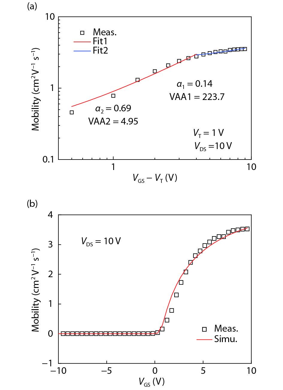
Fig. 1 shows the fitting curve of the extracted measured mobility (a), and the comparison of the measured and the simulated mobility (b) for IGZO TFTs. Actually, the fitting curve for log(μFE) to log(VGS – VT) isn’t continuous for the different operating regimes. Thus, besides the parameters shown in Eq. (5) (i.e. α, VAA, μ0), there are other shape related parameters for the accurate mobility modeling using RPI model (LEVEL 35)[
![]()
Figure 1.(Color online) (a) The fitting curve of the extracted measured mobility and (b) comparison of the measured and the simulated mobility for IGZO TFTs.
On the basis of the extracted mobility, by further tuning the physical parameters according to the TFT process, and properly adjusting the fitting parameters in the RPI models, excellent fitting can be obtained between the simulation and calculation results of drain-to-source current versus the gate-to-source voltage as shown in Fig. 2. However, due to the complicated leakage current path, there is still discrepancy in the backward leakage region. For practical AMOLED pixel operation, the IGZO TFTs mainly operate in the above-threshold and the near-threshold voltage regions, thus it is sufficiently accurate for the SPICE studies.
![]()
Figure 2.(Color online) The current-to-voltage curve of IGZO TFT with measured and simulated results.
3. Results and discussions
3.1. Pixel circuit descriptions
The investigated pixel schematic and the timing diagram are shown in Fig. 3. Being different from the previous timing diagram shown by Kawashima et al.[
On the other hand, there is no overlap between the VSCAN and VEM2 for the previous schematics. Then, the initializations for the left and right electrodes of CS take place for different time intervals. Although being pre-charged with VOLED + EVSS through the turned-on TEM, the source electrode of the driving transistor is prone to be disturbed by the following data input due to the voltage coupling effect of CS. In this case, the precision of VT extraction through the ‘source follower’ structure is reversely influenced. Thus, compared with the previous schematic, the proposed driving method has better programming and VT compensating ability.
The operating procedures of the investigated pixel circuit are divided into (1) initialization, (2) data input, and (3) light emitting, as shown in Fig. 3(b). The operating details are described as follows.
(1) Initialization
For this period, the voltage of VEM2 and VSCAN are high, and the level of VEM1 is low. Then, the switching transistors, i.e. TS0, TS1 and TEM2 are turned on. Consequently, the left and right electrodes of CS are charged with VDATA and VOLED + EVSS, respectively. The internal node G, i.e. the gate electrode of the driving transistor tD is charged with VREF through TS0.
(2) Data input
Then, the level of scan signal VSCAN is high, and the emit-controlling signals VEM1 and VEM2 are switched to low. Thus, the switching transistor TEM2 is turned off. Consequently, the source electrode of the driving transistor, i.e. the right terminal of the storage capacitance CS, is charged with VREF – VT. On the other hand, the data voltage is transferred to the left terminal of the storage capacitance CS. Thus, the voltage difference of (VDATA – VREF + VT) is programmed and stored by CS. In other words, the threshold voltage information of the driving transistor is stored by CS. This is a typical ‘source follower’ structure, and the analysis in this paper can also be applied to lots of other similar circuits.
(3) Light emitting
For the light emitting period, both the voltage of VEM1 and VEM2 are turned to high, and the voltage of the scan signal VSCAN is low. Thus, the stored charges in the capacitance CS are almost completely transferred to the gate electrode of the driving transistor. According to the charge conservation law, the gate-to-source voltage of TD can be expressed as [CS(VDATA - VREF + VT) + CGVREF]/(CS + CG), Here, CG is the total capacitance associated with gate electrode of the driving transistor. For practical pixel designs, CS
Here VS is the anode voltage of OLED with the turning-on state, which is approximately constant. So the analysis proves that the driving current for OLED of the demonstrated circuit is independent of threshold voltage of the driving transistor.
3.2. Mobility influence on the current error
As previously mentioned, the threshold voltage of the driving transistor is stored on the right terminal of storage capacitance CS, and the value of the voltage of the source electrode of the driving transistor is dependent on the charging procedure of the driving transistor for the data input period. Then, whether the mobility of IGZO TFT will have an influence on the extracted threshold voltage should be checked through transient analysis. Here, simulation investigations for the pixel circuit are carried out using SmartSpice and the design parameters of the proposed pixel clrcuit are listed in Table 2.
Fig. 4 demonstrates the simulated transient response of VS, VGS, and IOLED (a), and the voltage of node X(b), with the previous and the proposed driving method. It is shown that, the voltage of node X is almost the same for the previous and the proposed method for the initialization and data input phases, but there are derivations in the light emitting phase. For the previous timing scheme, due to the lack of proper initialization phase, the voltage of the source electrode of TD (i.e. VS) is prone to fluctuate with the input voltage, which results in the failure of programming of VGS and IOLED. These comparison results further prove the previously illustrated analysis.
![]()
Figure 3.(Color online) (a) IGZO TFT integrated AMOLED pixel circuit and (b) the timing diagram.
Fig. 5 shows the voltage of source electrode versus the mobility of IGZO TFT with the threshold voltage shift. Here, the source voltage is extracted at the end of the data input procedure. The mobility varies from 1 to 50 cm2V−1s−1 with the threshold-voltage shift from −1 to 1 V. It is observed that the extracted voltage of source electrode increases with the mobility due to the enhanced charging ability of driving transistor. But once the mobility is higher than 5 cm2V−1s−1, VS starts to saturate. This is because the loading capacitance at the source electrode of driving transistor is relatively small for the driving transistor. In the demonstrated pixel circuit, the driving transistor is isolated from the capacitance of OLED by the switching transistor TEM, which is controlled by VEM2. Then, for the ‘source follower’ structure, the loading capacitance of the threshold voltage extraction is relatively small. This is the main improvement of the discussed pixel circuit compared to the previous one[
![]()
Figure 4.(Color online) (a) The simulated transent response of
Fig. 6 shows the programmed current error with the driving current of 1 μA, for different threshold voltage shift. Here, the current error rate is defined as [IOLED(ΔVT)−IOLED(ΔVT = 0)])/IOLED(ΔVT = 0). It is observed that, for the mobility variation from 1 to 50 cm2V−1s−1, the compensating error is almost constant. The current error seems little large for high resolutions. For example, for a 6-bit resolution, the current error is required to be less than 1.56% (i.e. 2−6).This might be attributed to the large parasitic capacitance of back gate IGZO TFTs. Due to the voltage drop at the parasitic capacitance, the extracted threshold voltage cannot be accurately added to the gate-to-source voltage of the driving transistor as shown in Eq. (6). If new processes are adopted, such as top gate IGZO TFT with self-aligned source/drain, then it is possible that the programmed current error can be substantially decreased. To sum up, the influence of mobility on the current error isn’t so direct, and the current error cannot be decreased by merely increasing the mobility of IGZO TFTs.
![]()
Figure 5.(Color online) The source voltage of driving transistor with the increase of mobility for different threshold voltage shift.
3.3. Mobility influence on AMOLED layout
It is expected that, with higher effective mobility, the dimension of the TFT can be decreased. For the four switching transistors, i.e. TS0, TS1,TEM1 and TEM2, the dimensions are chosen to be the smallest, thus further increase of mobility is of no use. But for the driving transistor, the channel width can indeed be decreased, if increased mobility TFTs are used as shown in Eq. (6). Furthermore, the capacitance associated with the gate electrode of the driving transistor is decreased. According to the discussions in Section 2, the storing capacitance CS is determined by
where k is an empirical parameter. With the increase of k, the voltage loss due to the parasitic and the gate-to-channel capacitance can be neglected. Further, as IGZO TFTs own the merit of low-leakage current, the decreasing of CS is possible. In consequence, higher mobility benefits the decreasing of storing capacitance. According to the schematic of Fig. 3, the layout for proposed AMOLED pixel can be derived following the process rules[
![]()
Figure 6.(Color online) The programmed current error versus mobility for different threshold voltage shift.
![]()
Figure 7.(Color online) AMOLED pixel layout with mobility of (a) 10 and (b) 50 cm2V−1s−1.
4. Conclusion
In this paper, the influence of mobility on the performance of AMOLED pixel circuit with IGZO TFTs is investigated. The effective mobility is modeled and parameters for mobility and current-to-voltage characteristics are extracted to fit the measured electric performance of IGZO TFT samples. On the basis of the mobility model, a typical AMOLED pixel, which consists of 5 transistors and 1 capacitor with a new driving timing diagram, is investigated. In additions, the relationship between the pixel circuit performances on the mobility is demonstrated. It is shown that the compensation efficiency of threshold voltage is almost independent on the mobility of IGZO TFTs thanks to the isolation element of the ‘source follower’ structure and the OLED anode. While the storage capacitance can be decreased with higher mobility, and the pixel resolution is improved as a result. The demonstrated method and results is useful for the design of high performances AMOLED display panel with new metal oxide TFTs.
Acknowledgment
The author would like to thank the anonymous reviewers for their valuable suggestions. This work was supported by National Natural Science Foundation of China (No. 61404002) and the Shenzhen Municipal Scientific Program (No. JCYJ20150626111117384).
References
[1]
[2] C Leng, C Wang, L Wang et al. Separate frame compensated current-biased voltage-programmed active matrix organic light-emitting diode pixel. IEEE Electron Device Lett, 35, 847(2014).
[3]
[4] X Guo, S Silva. Investigation on the current nonuniformity in current-mode TFT active-matrix display pixel circuitry. IEEE Trans Electron Devices, 52, 2379(2005).
[5] X Guo, S Silva. A simple and effective approach to improve the output linearity of switched-current AMOLED pixel circuitry. IEEE Electron Device Lett, 28, 887(2007).
[6] M Wang, M Wong. An effective channel mobility-based analytical on-current model for polycrystalline silicon thin-film transistors. IEEE Trans Electron Devices, 54, 869(2007).
[7] A Nathan, A Kumar, K Sakariya et al. Amorphous silicon thin film transistor circuit integration for organic LED displays on glass and plastic. IEEE J Solid-State Circuits, 39, 1477(2004).
[8] A Nathan, S Lee, S Jeon et al. Amorphous oxide semiconductor TFTs for displays and imaging. IEEE J Display Technol, 10, 917(2014).
[9] X He, L Wang, X Xiao et al. Implementation of fully self-aligned homojunction double-gate a-IGZO TFTs. IEEE Electron Device Lett, 35, 927(2014).
[10] Y Kim, H Kang, G Kim et al. Improvement in device performance of vertical thin-film transistors using atomic layer deposited IGZO channel and polyimide spacer. IEEE Electron Device Lett, 38, 1387(2017).
[11] Y Tian, D Han, S Zhang et al. High-performance dual-layer channel indium gallium zinc oxide thin-film transistors fabricated in different oxygen contents at low temperature. Jpn J Appl Phys, 53, 04EF07(2014).
[12] A Kumar, A Nathan, G Jabbour. Does TFT mobility impact pixel size in AMOLED backplanes. IEEE Trans Electron Devices, 52, 2386(2005).
[13]
[14] M Estrada, A Cerdeira, A Ortiz-Conde et al. Extraction method for polycrystalline TFT above and below threshold model parameters. Solid-State Electron, 46, 2295(2002).
[15] P Servati, D Striakhilev, A Nathan. Above-threshold parameter extraction and modeling for amorphous silicon thin-film transistors. IEEE Trans Electron Devices, 50, 2227(2003).
[16] K Ryu, I Kymissis, V Bulovic et al. Direct extraction of mobility in pentacene OFETs using
[17] M Estrada, A Cerdeira, J Puigdollers et al. Accurate modeling and parameter extraction method for organic TFTs. Solid-State Electron, 49, 1009(2005).
[18]
[19]
[20]
[21] W Aerts, S Verlaak, P Heremans. Design of an organic pixel addressing circuit for an active-matrix OLED display. IEEE Trans Electron Devices, 49, 2124(2002).


Set citation alerts for the article
Please enter your email address

© Copyright 2018-2021 | Chinese Laser Press. All Rights Reserved 沪ICP备15018463号-20