
Shouqiang Lai, Shibiao Liu, Zilu Li, Zhening Zhang, Zhong Chen, Rong Zhang, Hao-Chung Kuo, Tingzhu Wu. Applications of lasers: A promising route toward low-cost fabrication of high-efficiency full-color micro-LED displays[J]. Opto-Electronic Science, 2023, 2(10): 230028
- Opto-Electronic Science
- Vol. 2, Issue 10, 230028 (2023)
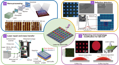
Fig. 1. The corresponding developments of laser applications in the fabrication processes of micro-LED full-color displays: (a ) Nano-processing, (b ) Defective detection, (c ) Laser repair and mass transfer, (d ) Patterning and morphology modification for QD-CCF. Figure reproduced with permission from: (a) ref.51, Optical Society of America, under a Creative Commons Attribution License; (b) ref.44, 52, Springer Nature, under a Creative Commons Attribution License; (c, d) ref.53, John Wiley and Sons, under a Creative Commons Attribution License.
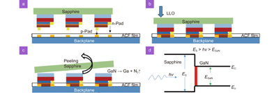
Fig. 2. (a –c ) Schematic of LLO process. (d ) Physical diagram of the LLO process.
Fig. 3. (a ) Schematic of the femtosecond laser LLO technology machining setup. (b ) The femtosecond laser LLO technology process, with single shots directed to the GaN surface for analysis of the beam characteristics shown on the left and the scanning pattern of the beam across the sapphire side in a uniform cross-pattern for lift-off experiments shown to the right. (c ) Microscopic images of the wafer and chip surface after applying the two-step LLO process with increasing laser power. Figures reproduced with permission from: (a–c) ref.66, John Wiley and Sons, under a Creative Commons Attribution License.
Fig. 4. (a ) PL intensity of good and defective chips detected by a micropulse laser. Inset: schematic illustrating adhesion is measured: after a 1.5 × 1.5 cm2 GaN piece on sapphire and a functional layer on a polyimide substrate are attached, the force generated by detaching these samples is measured. (b ) Mapping image of the detected PL intensity after micropulse laser irradiation. (c ) Optical microscopy image of defective chips on a real micro-LED wafer found using a PL intensity map. Figures reproduced with permission from: (a–c) ref.44, Springer Nature, under a Creative Commons Attribution License.
Fig. 5. (a ) SEM images of pixel damaged by dry etching. (b ) Electroluminescent images of the micro-LED array fabricated with 50 × 50 μm2 pixels and (c ) sketch of the laser-based micro-LED repair method. Figures reproduced with permission from: (a, b) ref.52, (c) ref.88, John Wiley and Sons, under a Creative Commons Attribution License.
Fig. 6. Process of mass transfer for micro-LEDs.
Fig. 7. Schematic of a brief chronology of the development of micro-LED displays and mass transfer techniques. Figures reproduced with permission from: ref.50, 85, 106,112, John Wiley and Sons, under a Creative Commons Attribution License; ref.85, Elsevier, under a Creative Commons Attribution License; ref.113, Optical Society of America, under a Creative Commons Attribution License; ref.114, IOP publishing, under a Creative Commons Attribution License.
Fig. 8. The principles of mass transfer technologies for micro-LEDs. (a ) Schematic illustration of a pick-and-place procedure via a stamp. (b ) Schematic of the Roll-to-roll contact micro transfer printing (µTP) process. (c ) An example of the specially designed micro-LED in a fluid self-assembly process. The navigation keel structure of LED chips ensures that the chips fall into the wells with the correct orientation aligned by torque forces. (d ) Schematic of the laser-induced forward transfer process. Figures reproduced with permission from: (a) ref.119, Royal Society of Chemistry, under a Creative Commons Attribution License; (b) ref.31, Springer Nature, under a Creative Commons Attribution License; (c) ref.50, John Wiley and Sons, under a Creative Commons Attribution License; (d) ref.113, Elsevier, under a Creative Commons Attribution License.
Fig. 9. Schematic of the principles of LIFT, LDW, tmSLADT and SLLO mass-transfer technologies.
Fig. 10. (a ) Process flow of laser-based SITRAB and (b ) tiling SITRAB process. Figures reproduced with permission from ref.135, John Wiley and Sons, under a Creative Commons Attribution License.
Fig. 11. Sketch of the laser ablation-based LEAP mass transfer processes. (a ) The LIFT process with the “donor” consists of a transparent substrate coated with a thin metal layer to be printed. A focused laser pulse is absorbed in the metal layer leading to local heating, and the resulting pressure at the interface provides the conditions for the transfer of the “flyer” part of the layer material. Finally, the transferred pixel land on the receiver. (b ) tmSLADT with a DRL: the explosion of the DRL provides the driving force of the material transfer. (c ) Schematic of LIFT of fluids: the laser pulse evaporates the solvent, which forms a gas bubble whose radius increases until its pressure equals the ambient pressure. Finally, the bubble collapses and a droplet separates from the jet filament.
Fig. 12. Schematic of laser-induced backward transfer with (a ) unstructured carrier during LIBT and (b ) structured carrier after transfer. Figures reproduced with permission from: (a-b) Ref.110, Elsevier, under a Creative Commons Attribution License.
Fig. 13. (a ) Schematic diagram of laser thermal releasing. (b ) Double-layer dynamic release layer structure. Figures reproduced with permission from: (a) Ref.115, John Wiley and Sons, under a Creative Commons Attribution License.
Fig. 14. (a ) Schematic of laser driven micro transfer placement technology. (b ) Schematic of i) programmable transfer printing platform; ii) microscopic photography of the steel ball selectively heated by the laser beam; iii–v) programmable transfer printing of silicon chips to a microstructured PDMS substrate; vi) the printed LED chip is lighted by a multimeter. Figure reproduced with permission from ref.114, John Wiley and Sons, under a Creative Commons Attribution License.
Fig. 15. (a ) Structure of ABX3 lead halide perovskite. (b ) Laser equipment of lead halide perovskite. (c ) Laser causes perovskite phase transition. (d ) Laser irradiation controls the film. (e ) Laser irradiation changes the grain size of perovskite. (f ) Laser annealing. (g ) Laser direct writing process and patterning example. (h ) Laser irradiation passivate perovskite defects. Figure reproduced with permission from: (b) ref.150, American Chemical Society, under a Creative Commons Attribution License; (c) ref.151, AIP Publishing, under a Creative Commons Attribution License; (d) ref.152, AIP Publishing, under a Creative Commons Attribution License; (e) ref.153,, American Chemical Society, under a Creative Commons Attribution License; (f) ref.154, MDPI Publishing, under a Creative Commons Attribution License; (g) ref.155, John Wiley and Sons, under a Creative Commons Attribution License; (h) ref.156, American Chemical Society, under a Creative Commons Attribution License.
|
Table 0. Comparison of laser-based mass transfer technology.
|
Table 0. Comparison of mass transfer technologies.
| ||||||||||||||||||||||||||||||||||||||||||||||||||||||||||||||||||||||||||||||||||||||||
Table 0. Progress of micro-LEDs and their applications.


Set citation alerts for the article
Please enter your email address

© Copyright 2018-2021 | Chinese Laser Press. All Rights Reserved 沪ICP备15018463号-20