1National Integrated Circuit Industry and Education Integration Innovation Platform, Department of Electronic Science, Xiamen University, Xiamen 361005, China
2Innovation Laboratory for Sciences and Technologies of Energy Materials of Fujian Province (IKKEM), Xiamen 361005, China
3College of Electrical and Computer Engineering, Yang Ming Chiao Tung University, Hsinchu 30010, Taiwan, China
4Semiconductor Research Center, Hon Hai Research Institute, Taipei 11492, Taiwan, China
Micro-light-emitting diodes (micro-LEDs) with outstanding performance are promising candidates for next-generation displays. To achieve the application of high-resolution displays such as meta-displays, virtual reality, and wearable electronics, the size of LEDs must be reduced to the micro-scale. Thus, traditional technology cannot meet the demand during the processing of micro-LEDs. Recently, lasers with short-duration pulses have attracted attention because of their unique advantages during micro-LED processing such as noncontact processing, adjustable energy and speed of the laser beam, no cutting force acting on the devices, high efficiency, and low cost. Herein, we review the techniques and principles of laser-based technologies for micro-LED displays, including chip dicing, geometry shaping, annealing, laser-assisted bonding, laser lift-off, defect detection, laser repair, mass transfer, and optimization of quantum dot color conversion films. Moreover, the future prospects and challenges of laser-based techniques for micro-LED displays are discussed.
Recently, micro-light-emitting diode (micro-LED) displays that reduce the size of traditional GaN-based LEDs to the micro-scale (smaller than 50 × 50 μm2), remove the sapphire substrate, and array the chips into drive-controlled pixels have been regarded as next-generation display technology and have attracted significant attention1-3. Compared with liquid crystal displays and organic LED technology, the self-luminous display technology of micro-LEDs has many advantages, such as low power consumption, fast responses, long lifetimes, and high efficiency; another feature of micro-LEDs is their application in high-resolution display panels. Micro-LEDs present great potential in many photoelectric fields, such as virtual reality (VR)/augmented reality (AR) light engines, smart watches, and high-resolution televisions. In the field of communication, micro-LEDs are also suitable for the application of visible light communication (VLC) and underwater optical communication4-11. The significant potential of micro-LEDs in the consumer electronics market has evoked enthusiasm among researchers. However, although micro-LEDs have exhibited excellent performance in various fields, there remain multiple challenges to their commercialization. For example, traditional technology cannot meet the demand for processing micrometer-sized devices, as the manufacturing process of inductively coupled plasma reactive ion etching (ICP-RIE), which is used to define and form the pixel, introduces sidewall defects; thus, it deteriorates the production yield and luminous efficiency of micro-LED displays12, 13. In addition, traditional detection and mass-transfer techniques result in prohibitive manufacturing costs, and the industrialization technology of full-color displays based on micro-LEDs is not yet fully mature14-17. These challenges have hindered the commercialization of full-color micro-LED displays.
Table Infomation Is Not Enable
Since Bell Labs in the United States proposed microdisk laser technology in 1992, micro-scale photoelectronic devices have attracted great attention18. H. X. Jiang et al. first prepared GaN-based micro-LEDs in 2000 and successfully fabricated a 10 × 10 blue micro-LED array with a diameter of about 12 μm in 200119, 20. In 2004, M. D. Dawson et al. reported the fabrication process and performance of a 64 × 64 array of ultraviolet (UV) micro-LEDs with a diameter of about 20 μm21. K. M. Lau and Z. J. Liu et al. reported on UV and red, green, and blue (RGB) micro-LEDs with a diameter of 50 μm and 360 pixels per inch (PPI) resolution in 201322, and then on blue micro-LEDs with 1700 and 2500 PPI resolution displays23, 24. In 2014, P. F. Tian et al. fabricated 10 × 10 micro-LED arrays with pixel diameters of 45 μm and peak emission at ~470 nm25. In 2016, B. Liu et al. developed a new type of hybrid nanohole periodic array/II-VI group white light LED, which used dipole coupling to enhance the nonradiative-energy transfer mechanism to achieve white light emission, exhibited high color conversion efficiency and effective quantum yield, and obtained an ultra-high color rendering index26. In 2019, F. Y. Jiang and N. Chi et al. proposed micro-LEDs fabricated on Si for applications in the field of underwater VLC27. In 2020, J. Han et al. fabricated semi-polar green micro-LEDs, which improved the efficiency and bandwidth of micro-LEDs in display and VLC applications28. In 2021, H. C. Kuo and T. Z. Wu et al. proposed a flexible white-light system for high-speed VLC applications, which consisted of a semi-polar blue InGaN/GaN single quantum well micro-LEDs on a flexible substrate of green CsPbBr3 perovskite quantum dot (PQD) and red CdSe quantum dot (QD) papers29. In 2022, M. D. Dawson et al. proposed an ultrahigh frame rate digital light projector using chip-scale micro-LEDs on a complementary metal–oxide–semiconductor (CMOS), in which a self-emissive chip-scale projector system based on micro-LEDs was directly bonded to a smart pixel CMOS drive chip. Therefore, the micro-LED arrays could project binary patterns at up to 0.5 Mfps and toggle between two stored frames at megahertz speeds. This technology can be used in conjunction with high-speed spatial pattern projection30. Research into micro-LEDs for applications in displays and communication since 2000 is summarized in Table 1.
Decreasing chip size leads to greater stress, defect density, wavelength, and brightness uniformity requirements for the epitaxial growth of wafers for micro-LEDs. When these requirements are not met, defective pixels must be detected and repaired effectively to yield pixels that achieve 99.999% in full-color micro-LED displays31, 32. In addition, because the size of the light-emitting surface of micro-LEDs is smaller in relation to their thickness, efficient and nondestructive techniques for substrate lift-off and annealing technology with high precision, high efficiency for temperature and area control are needed33, 34. Moreover, millions of micro-LEDs are available for display applications. Thus, a bottleneck of mass-transfer techniques hinders the practical application of micro-LEDs, necessitating the optimization of traditional mass-transfer technology35, 36. In addition, the preparation of color-conversion layers for full-color micro-LED displays faces many challenges, such as the patterning and morphology modification of the quantum-dot color conversion films (QD-CCF)37. In conclusion, the processing, detection, repair, mass transfer, and full-color technology of full-color micro-LED displays with the advantages of low cost, high precision, and high production efficiency are essential.
Recently, laser-based technology has attracted attention for its advantages in the preparation of full-color micro-LED displays. For example, in 2023, ASMPT launched a new type of laser-based device for the mass transfer of micro-LEDs38. Simultaneously, Xiamen University built the world’s first 23.5-inch laser-based mass-transfer production line of micro-LEDs39. In addition, “Touch Taiwan Smart Display” reported that 2023 is the first year of micro-LED mass production40… Unlike traditional processes, laser-based processes have the advantages of no contact, adjustable energy, high speed, and high material selectivity in the multi-material system and no cutting force acting on the device. The application of lasers during micro-LED processing is shown in Fig. 1. Lasers can be used in chip dicing, geometric shaping, annealing, bonding, and lift off. For example, Gu et al. used a repetitively pulsed UV copper vapor laser (255 nm) to manufacture and dice micro-LEDs in 200441, Guo et al. used picosecond laser multiple scribing to shape the substrate sidewalls of LEDs42, and Zheng et al. used laser annealing to optimize the contact resistance of Mg-doped GaN43. In addition, lasers with short wavelengths can be used for the photoluminescence (PL) detection of micro-LEDs, which can distinguish sub-standard devices, thus improving the yield during mass transfer and effectively reducing the cost of laser repair. For example, Park et al. used a 375-nm micropulse laser to detect the properties of micro-LED arrays44. Owing to their high precision, high efficiency, and low cost, lasers can be used in the repair and mass-transfer procedures of micro-LEDs. For example, the laser repair and laser-enabled advanced placement (LEAP) mass-transfer strategies, which use the beam-addressed release (BAR) method, selectively release perfect micro-LEDs with the advantages of large size, no contact, and high efficiency45. Moreover, super-inkjet printing technology for QDs patterning can produce 1732 PPI full-color displays46. With the widespread application of lasers, the commercialization of full-color micro-LED displays has been vigorously promoted.
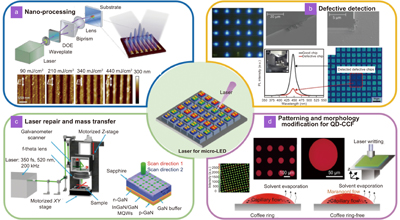
Figure 1.The corresponding developments of laser applications in the fabrication processes of micro-LED full-color displays: (a) Nano-processing, (b) Defective detection, (c) Laser repair and mass transfer, (d) Patterning and morphology modification for QD-CCF. Figure reproduced with permission from: (a) ref.51, Optical Society of America, under a Creative Commons Attribution License; (b) ref.44, 52, Springer Nature, under a Creative Commons Attribution License; (c, d) ref.53, John Wiley and Sons, under a Creative Commons Attribution License.
In recent years, several problems associated with the application of micro-LED displays have been identified. In 2020, P. F. Tian and H. C. Kuo et al. reviewed micro-LED mass transfer technology47. In 2021, B. Shen et al. summarized the problems with and possible solutions to the epitaxial growth and chip technology of micro-LED displays48. In 2022, M. J. Cheng et al. categorized the mass transfer, detection, and repair technologies for micro-LED displays31. In 2022, H. C. Kuo et al. summarized the application progress and future development of QD-based full-color micro-LED displays49. These summaries considerably improve the understanding on micro-LED display technologies. However, few studies have focused on laser-based technologies for micro-LED displays. This review comprehensively analyzes the challenges surrounding micro-LED displays, including fabrication problems such as processing, detection, repair, mass transfer, and QD-based full-color displays. In addition, the applications of laser-based technologies and future development trends in the fabrication of micro-LEDs are discussed50-53.
Overview of micro-LED-based full-color displays
Challenges in full-color micro-LED displays
The reduced size of micro-LEDs optimizes their junction temperature and current density distribution. However, as the size of micro-LEDs decreases, their large volume-to-surface ratio results in the generation of sidewall defects and surface damage caused by dry etching via ICP-RIE. The problems of conductivity control and electrode structure design in the device would lead to the longitudinal expansion of current, which in turn results in current crowding effect in micro-LEDs. In addition, the uneven luminescence distribution and excessively large light angle of micro-LEDs would cause light crosstalk in displays54-57. These factors deteriorate the efficiency and reliability of the devices. Therefore, optimizing techniques for sidewall passivation, improving the current-crowded effect, and reducing optical crosstalk between pixels are necessary in fabricating micro-LED devices58-60. In addition, for the yield of micro-LED displays to exceed 99.999%, defective pixels generated during fabrication and mass transfer should be accurately detected, removed, and repaired. Mass transfer is also a challenge for full-color micro-LED displays. The ultrahigh yield requirement for RGB micro-LEDs and fabrication bottleneck for red micro-LEDs result in high cost, which hinders the development and application of full-color micro-LED displays61, 62. An alternate method to achieve full-color displays is using QD-CCF technology; the patterning and morphology modification of QD-CCF help reduce optical crosstalk and improve the efficiency, resolution, and reliability of full-color micro-LED displays63, 64. In this case, the fabrication of micro-LEDs includes the epitaxial growth of wafers, device preparation, defect detection, defect repair, mass transfer, and full-color displays, which should be improved to achieve the commercialization of micro-LED displays65-71.
Advantages of lasers for fabricating micro-LEDs
Lasers have been employed as an effective tool for micromachining and afford versatile methods for cutting, drilling, and modification of various engineering materials owing to their directionality, uniform wavelength coherence, and high energy density72. During the fabrication of micro-LEDs, parameters such as laser intensity, wavelength, and pulse duration can be changed; thus, laser processing technology differs from traditional processing technologies. The unique advantages of laser-based technologies for fabrication of micro-LEDs are noncontact processing, adjustable laser beam energy, high efficiency, and low cost73.
Laser-based processing technology for micro-LEDs
The increasing demand for micro-LEDs has driven the development of related processing technologies. Advanced technologies such as laser-based wafer dicing, geometry shaping, laser-assisted bonding, and laser lift-off (LLO) have been proposed and developed to optimize the production yield, efficiency, and cost during the manufacturing of micro-LEDs.
Wafer dicing
As regards the manufacturing of micro-LEDs, ultrahigh hardness of sapphire can cause issues such as low yield, low output, and high cost74. Traditional diamond dicing technology only achieves row widths of 50 μm, which is comparable to the size of micro-LEDs. Similarly, the low-cost and high-speed plasma dicing technology faces the challenges of low dicing accuracy and excessively large dicing grooves in addition to generating harmful gases and arcs during the dicing processes. Unlike traditional diamond dicing and plasma dicing methods, the accuracy of UV lasers achieves a row width of 2.5–20 μm, which would allow for significant increase in the production yield of micro-LEDs75. In addition, the LEDs exhibit no significant brightness loss, and the increased absorption rate of GaN and sapphire to short-wavelength light from UV lasers helps reduce the radiant power required for dicing. Moreover, the processing efficiency is also improved significantly. In this case, UV lasers are considered ideal tools for wafer dicing76, 77. These techniques are discussed in the following sections.
Geometry shaping
To enhance the light extraction efficiency (LEE) of LEDs, wet etching, plasma etching, and laser-based geometry shaping techniques have been employed. While wet etching has the advantage of being low cost and highly efficient, the use of strong acids and alkalis for etching GaN is associated with a high health hazard risk. Further, the accuracy of the etching process is insufficient. Plasma etching technology has similar advantages of low cost, low pollution, and high etching rate. However, the poor anisotropy of plasma etching causes serious drilling erosion, and the accompanied glow discharge during the processing procedures hinders its application in micro-LED geometry shaping. Therefore, wet etching and plasma etching are only suitable for processing the geometry shape of the entire micro-LED. In contrast, laser-based geometry shaping technology has the advantages of high controllability, high accuracy and high efficiency; therefore, the electrical characteristics of the devices would not deteriorate, and this technology is applicable in the nanostructure processing of micro-LEDs78-80. Fu et al. reported a single-step dicing and shaping method for InGaN-based LED chips using a laser micromachine; chips shaped into inverted pyramids presented an 85.2% increase in LEE81. Lin et al. fabricated InGaN-based LEDs with cone- and sawtooth-shaped sapphire sidewall structures using a laser drilling process in which the light output power was 16% higher than that of a conventional LED structure with a laser-scribed sidewall82. To overcome the problems of debris and contaminants generated during geometry shaping, picosecond lasers have been used instead of nanosecond lasers. For example, Lin et al. performed laser decomposition, laser scribing, and lateral crystallographic wet etching at the GaN/Al2O3 interface to form LEDs with a rough-patterned back on the N-face GaN surface83. Guo et al. proposed a ps-laser dicing method to form LEDs with oblique substrate sidewalls. During processing, the applied multiple scribing lines in the sapphire were intentionally aligned to guide the wafer to be diced along the oblique sidewalls with designed angles42. Li et al. proposed parallel laser processing technologies that can fabricate functional devices such as LEDs, photovoltaic devices, light sensors, and optical components or windows as micro/nanostructures of gratings, pyramids, porous structures, rods, and cones over a large area with high efficiency84.
Laser lift-off
The lattice mismatch between Group III nitrides and sapphire causes strong compressive stress, which leads to a large defect density and a strong quantum-confined Stark effect in micro-LEDs85. Moreover, the poor thermal and electrical conductivity of sapphire lead to poor heat dissipation and high resistance in micro-LED displays, which hinders the development of applications; thus, it is necessary to develop techniques that are used for the lift-off of micro-LEDs from sapphire86. Currently, three popular lift-off methods have attracted attention87: LLO, chemical and mechanical lift-off (CLO), and spalling. However, CLO technology faces many challenges, such as chemical pollution and high cost, and spalling technology has many drawbacks and limitations owing to the hardness of the sapphire substrate and its wurtzite crystal lattice88, 89. LLO technology, which environmentally heats the crystal and causes damage to achieve high throughput and yield without sacrificing the wafer area, has overcome many problems associated with standard separation techniques and is therefore the most promising technology for micro-LEDs90.
Currently, the excimer nanosecond pulse lasers and ultrafast pulse lasers have been proposed for LLO. Compared with excimer nanosecond pulse lasers, ultrafast lasers with a pulse within 10−11 s and appropriate lift-off single pulse energy could reduce the thermal damage during LLO processes. Thus, these lasers are expected to become a key breakthrough point in the bottleneck of micro-LED mass transfer91, 92. The chemical equation of laser-induced thermal decomposition of GaN is as follows93:
The schematic and physical mechanism of the LLO processes is depicted in Fig. 2(a–d), for bandgap energies of 9.2 and 3.3 eV of sapphire and GaN, respectively; therefore, lasers with a wavelength lower than the absorption edge of GaN (such as the 248-nm (5.0 eV) KrF excimer nanosecond pulse laser) could be used to decompose the material of GaN. The LLO process is as follows. A short-wavelength pulse laser is used to decompose the micro-GaN into N2 and Ga. This significantly weakens the interface adhesion between the sapphire substrate micro-LED, allowing for the sapphire to be released by remelting or etching the metal94, 95.
Figure 2.(a–c) Schematic of LLO process. (d) Physical diagram of the LLO process.
Many methods for improving the efficiency and validity of LLO have been proposed. An example is the step-and-repeat method, which refers to the process of spot scanning line by line until the entire area is scanned. During scanning, adjusting the size and step of light spots is necessary to make good connections between them and avoid damage caused by repeated scanning and overlapping light spots. With regard to the lift-off of micro-LEDs using diode-pumped solid state (DPSS) lasers (DPSS), the line-by-line scanning method results in an uneven stress release during LLO, which leads to an excessive curvature of the wafer and possible dark cracks or fragments. The spiral scanning method, which moves from the periphery to the center of the wafer, was proposed to achieve a uniform stress release and reduce the warpage of the wafer after LLO. Moreover, the femtosecond laser LLO technology for the production of free-standing GaN light-emitting diode chips has been developed. The laser machining setup is illustrated in Fig. 3(a). As shown in Fig. 3(b), by using the high-energy pulsed laser beam to penetrate the sapphire substrate and to evenly scan the interface between the sapphire substrate and the epitaxial GaN material, the separation of the substrate and chips could be achieved. In addition, microscopic images of the wafer and chip surface after applying the two-step LLO process with increasing laser power are shown in Fig. 3(c)66.
Figure 3.(a) Schematic of the femtosecond laser LLO technology machining setup. (b) The femtosecond laser LLO technology process, with single shots directed to the GaN surface for analysis of the beam characteristics shown on the left and the scanning pattern of the beam across the sapphire side in a uniform cross-pattern for lift-off experiments shown to the right. (c) Microscopic images of the wafer and chip surface after applying the two-step LLO process with increasing laser power. Figures reproduced with permission from: (a–c) ref.66, John Wiley and Sons, under a Creative Commons Attribution License.
The application of micro-scale chips in consumer electronics, connected hardware, electronic medical equipment, and other fields faces the challenges of high-efficiency detection, location, and removal of defects. However, technologies such as spectral detection, spectral correction, automatic detection, and deep learning have emerged to improve the sensitivity and accuracy of defective chips. In the display field, micro-LEDs are regarded as next-generation display technology that requires a yield exceeding 99.999%. Therefore, defective pixels caused by fabrication and mass transfer processes should be accurately detected and removed96-98.
The luminous intensity and uniformity of micro-LEDs are essential for performance, such as that of the color gamut and brightness; thus, defect detection technologies have practical significance in industrialization. Traditional cathodoluminescence defect detection technology damages the characteristics of micro-LEDs, and the efficiency of electroluminescence (EL) defect detection technology is not applicable to industrialization. Therefore, the PL defect detection technique using lasers with the advantage of no contact and ultrahigh detection efficiencies has attracted attention. This technology applies a specific laser irradiation wavelength onto micro-LEDs; the characteristics of the micro-LEDs obtained from this PL spectrum can be used for screening. Figure 4(a) shows the high-efficiency micro-PL scan obtained with the pulsed laser beam on the wafer containing the micro-LED. As shown in Fig. 4(b, c), the defective chip could be quickly located using the laser inspection system by measuring the PL intensity of micro-LEDs. The PL intensity of the good chip and the PL intensity of the defective chip are shown in Fig. 4(a)44.
Figure 4.(a) PL intensity of good and defective chips detected by a micropulse laser. Inset: schematic illustrating adhesion is measured: after a 1.5 × 1.5 cm2 GaN piece on sapphire and a functional layer on a polyimide substrate are attached, the force generated by detaching these samples is measured. (b) Mapping image of the detected PL intensity after micropulse laser irradiation. (c) Optical microscopy image of defective chips on a real micro-LED wafer found using a PL intensity map. Figures reproduced with permission from: (a–c) ref.44, Springer Nature, under a Creative Commons Attribution License.
Laser repair technology and mass transfer strategies
Laser repair technology
The yield requirement for full-color micro-LED displays should exceed 99.999%. However, traditional repair technologies for micro-devices demand considerable human and material resources, and the low efficiency and unavoidable artificial errors during this process result in a low product yield. Thus, laser repair technology, which has the advantages of adjustable light output power, spot size, and penetration depth, has attracted great attention in the manufacturing of full-color micro-LED displays. Additional challenges include the fracture of metal electrodes, poor contact, and damage to chips during manufacturing. Therefore, laser-based metal melting or cladding and the replacement of damaged micro-LED pixels are in demand.
Using lasers with a high power density, metal surfaces can be heated and melted. Subsequently, through the rapid heat conduction and heat flow modes of the material matrix, the melting metals can be quickly solidified to repair cracked electrodes. For example, Gui et al.99 used the laser direct writing technology to fabricate nanoscale Ni/Au wire grids as transparent conductive electrodes in LEDs. Kuntoglu et al.100 proposed developing an advanced and efficient method for the surface treatment of coatings; this method would adjust the process parameters of coatings, improve the absorption coefficient of the material matrix, increase the cooling rate of molten metal, improve the hardening effect, and reduce the residual stress in materials. To avoid burning loss (component segregation caused by the uneven distribution of elements), Zhang et al.101 used the laser-melting technology to investigate the effects of aging temperature and aging time on the microstructure, mechanical properties, and corrosion resistance of the metal alloys. Laser-cladding can achieve an improved material strength, greater beam area, lower cost, and better thermal fatigue resistance owing to the combination of the matrix and powder. For example, Gnanamuthu et al.102 first proposed the laser cladding technique on a metal matrix, which could be used to repair chips, Imam proposed a spatial damage positioning method in laser repair processes using an autonomous robot103. Therefore, laser melting or cladding technologies are suitable for the repair of micro-LED displays, owing to their advantages of low cost, high stability, and excellent electrode repair effects.
In addition to electrode breakage and the poor contact of defective micro-LEDs, as well as the accuracy of fabrication processes, such as lithography and ICP-RIE, can also reduce the performance. However, it is difficult and expensive to improve the performance of damaged micro-LEDs; thus replacing damaged pixels with qualified devices in the display module is a superior alternative. To prevent the micro-LEDs in the undamaged area from being affected, the location of the damaged or missing micro-LEDs should be accurately detected during the laser repairing process. Laser parameters, such as power density and laser spot size should therefore be controlled. In addition, a high-precision visual detection system must be employed to determine the coordinates of the defective micro-LEDs so as to satisfy the ultrahigh requirements of the detection algorithm in an advanced repair machine. The PL based laser detection system could capture the emitted photoluminescence and create images or maps of the material under inspection. Consequently, the damaged or missing micro-LEDs could be identified and located by using the signal processing algorithms or image enhancement methods to improve the visibility of defect regions. To address these challenges, Taha et al. proposed a defect detection method based on the spatial dependence of the defect pattern104. The method clusters patterns of defective chips according to their spatial dependence across all wafer diagrams and identifies the most dominant defect patterns on the wafer. Bai et al. proposed an advanced vision repair algorithm with adjustable detection speed and accuracy function on the XY-axis105. With noncontact micropulse laser scanning technology, micro-LEDs can be excited with a high-energy focusing laser beam, and the differences in PL signals can be obtained and analyzed; thus, the position of defective micro-LEDs can be detected. Once the defective micro-LEDs are identified and located, it is essential to remove and replace the defective chips. Cok et al. proposed a redundant pixel design method that places parallel-connected redundant pixels; the redundant pixels replace the function of damaged pixels106. Park et al. proposed a stamp transfer technique with significant advantages, such as high efficiency, high accuracy, and no damage to the micro-LED44. However, laser trimming and re-bonding technologies have been regarded as the most promising methods. Laser trimming technology melts and evaporates the focused surface area of materials in which defective micro-LEDs are located; the defective micro-LEDs are trimmed using lasers and glued at the corresponding position using the re-gluing method. In addition, the laser-assisted bonding with compression process proposed by Choi et al. completes the adhesion of the micro-LED array, thus proving the feasibility of repair107. Moreover, Choi et al. also verified the feasibility of laser-assisted bonding, which has attracted considerable attention owing to its low-carbon and environmental protection characteristics107-109. Figure 5 shows the scanning electron microscope (SEM) and electroluminescent images of defective chips and the sketch of the laser-based micro-LED repair method52, 88. Figure 5(b) shows an array with both active and inactive pixels. The initial process depicted in Fig. 5(c) seeks to locate the position of defective pixels and remove all defective pixels through the laser trimming process. Then, according to the location of the damaged bare chip, a separate process is used to assemble the micro-LED onto a temporary carrier.
Figure 5.(a) SEM images of pixel damaged by dry etching. (b) Electroluminescent images of the micro-LED array fabricated with 50 × 50 μm2 pixels and (c) sketch of the laser-based micro-LED repair method. Figures reproduced with permission from: (a, b) ref.52, (c) ref.88, John Wiley and Sons, under a Creative Commons Attribution License.
Mass transfer typically refers to the diffusion and convection of a large number of molecules or particles from one region to another. In the field of micro-LEDs, mass transfer technology, which requires the transfer of millions of micro-LEDs from sapphire to another substrate or a drive circuit board using high-precision equipment, has promoted the development of many technologies, such as pick-and-place, fluid self-assembly (FSA), and laser-based mass transfer, etc. However, these technologies involve two processes, as shown in Fig. 6: substrate separation and chip take-up. The specific transfer process is as follows: (a) substrate separation, in which the chip is separated from the source substrate by force; and (b) substrate transfer, in which the separated micro-LED chips are transferred from the source substrate to a specific position on the target substrate with high precision using the transfer equipment.
Two bottlenecks hinder the development of micro-LED mass transfer. First, the thickness of the epitaxial layer of micro-LEDs is only 3% that of traditional LEDs; for smaller micro-LEDs, ultrahigh precision transfer is required. Second, the transfer of millions of micro-LEDs requires high transfer efficiency; thus, traditional methods with low transfer efficiency, low accuracy, and high cost cannot meet the requirements of micro-LEDs111. Researchers have proposed many strategies to achieve a high-yield and low-cost fabrication of micro-LED-based displays. The development of mass transfer technology for micro-LEDs is shown in Fig. 750, 85, 106, 112-115.
Figure 7.Schematic of a brief chronology of the development of micro-LED displays and mass transfer techniques. Figures reproduced with permission from: ref.50, 85, 106,112, John Wiley and Sons, under a Creative Commons Attribution License; ref.85, Elsevier, under a Creative Commons Attribution License; ref.113, Optical Society of America, under a Creative Commons Attribution License; ref.114, IOP publishing, under a Creative Commons Attribution License.
The principles of mass transfer technologies, including stamp transfer printing, Roll-to-roll transfer, FSA mass transfer, and laser-induced forward transfer (LIFT) technologies, are illustrated in Fig. 8116-119. The pick-and-place technology operates under the mechanical principle of van der Waals, as well as electrostatic and electromagnetic forces. The micro-LEDs can be picked up and placed using the transfer head. The pick-and-place technology can be classified into electrostatic stamp, magnetic stamp, elastomer stamp, and roll-to-roll based on the applied force during the process. In addition, mass transfer efficiency is related to the size of the transfer head. However, there are many requirements for micro-LEDs during the pick-and-place process. For example, micro-LEDs should be incorporated with iron or nickel during the magnetic stamping, and bridges should be fabricated between micro-LEDs and the substrate during electrostatic, magnetic and elastomer stamping, which affect the electroluminescence properties of micro-LEDs118, 119. For representative FSA mass transfer technologies, such as magnetic and FSA, the process is as follows: while placing a large number of micro-LEDs in the system, the magnetic or fluid forces move the micro-LEDs at a specified speed and then counter-assemble them with the substrate120. FSA mass transfer technologies have the advantages of high efficiency and low cost121. However, it is difficult to control the fluid force, and the yield of micro-LEDs using FSA technology is low, which increases the complexity and cost of defect repair122. Owing to their distinct advantages of high efficiency, good selectivity, and high yield, two-dimensional materials-based layer transfer (2DLT) and laser-driven transfer technologies are prospects for industrialization. The 2DLT technology, which could achieve a top-down fabrication to yield vertical RGB micro-LEDs, allows for epitaxy of ultrathin RGB LEDs onto 2D material-coated substrates via either remote or van der Waals epitaxy. The process is followed by the mechanical release of LED layers from 2D materials, subsequent reuse of the substrate and stacking of these micro-LEDs via the use of adhesive polymer layers123. As for the laser-based mass transfer, there are chemical and physical interactions between the laser beam and films, which generate force to transfer the micro-LEDs because of ablation or heat release. Selective transfer can be achieved through the mask or focusing spot arrays, which have great advantages for defect repair. Uniqarta, Coherent and QMAT LTD. has proposed a laser-based LIFT technology, which can achieve an ultrahigh transfer efficiency of 100 million units per hour124. The micro-LEDs can be transferred to non-flat substrates without affecting their operational characteristics and the distance between each chip (chip spacing) has the potential to be extremely small as compared to other mass transfer technologies. Therefore, 2DLT and laser-driven transfer are considered as the most promising micro-LED mass transfer technologies. A comparison of mass transfer strategies is summarized in Table 2.
Figure 8.The principles of mass transfer technologies for micro-LEDs. (a) Schematic illustration of a pick-and-place procedure via a stamp. (b) Schematic of the Roll-to-roll contact micro transfer printing (µTP) process. (c) An example of the specially designed micro-LED in a fluid self-assembly process. The navigation keel structure of LED chips ensures that the chips fall into the wells with the correct orientation aligned by torque forces. (d) Schematic of the laser-induced forward transfer process. Figures reproduced with permission from: (a) ref.119, Royal Society of Chemistry, under a Creative Commons Attribution License; (b) ref.31, Springer Nature, under a Creative Commons Attribution License; (c) ref.50, John Wiley and Sons, under a Creative Commons Attribution License; (d) ref.113, Elsevier, under a Creative Commons Attribution License.
With the development of new technologies, lasers have become an indispensable industrial tool for “tool-free” high-precision manufacturing. In 1972, Kontrowitz et al. proposed a laser propulsion technology that uses UV photons to excite electrons, resulting in the ablative decomposition of materials, and infrared photons to realize electron vibrational and rotational excitation, leading to thermal decomposition. Traditional stamping methods are affected by differences in the modulus of elasticity, heat conduction, and thermal expansion of materials. Therefore, the noncontact advantages of laser-assisted mass transfer remarkably broaden its application range125-129. Laser-based mass transfer involves picking up micro-LEDs using a transfer head and selectively transferring micro-LEDs using laser irradiation. Inserting a sacrificial layer of photothermal material between the chip and the transparent substrate is necessary for the protection of the micro-LEDs. Laser-based mass transfer technologies can be divided into laser ablation and direct laser thermal release. During the laser ablation mass transfer process, the sacrificed layer is ablated under the laser irradiations, and the generated gas impacts the chip, thus releasing and transferring micro-LEDs. Direct laser thermal release refers to the thermal decomposition of the intermediate material under the laser irradiation, which detaches and transfers the micro-LEDs. Figure 9 shows the principle of LIFT, laser direct writing (LDW), thermomechanical selective laser-assisted die transfer (tmSLADT), and selective laser lift-off (SLLO) mass-transfer technologies; detailed comparisons are listed in Table 3.
Figure 9.Schematic of the principles of LIFT, LDW, tmSLADT and SLLO mass-transfer technologies.
Laser ablation of GaN leads to Ga deposition and gas generation. The deposition of Ga can be cleaned with water or diluted hydrochloric acid, and the generation of gas, which could impact the micro-LEDs, results in the separation of chips and the substrate, thus realizing mass transfer. Based on the above principles, significant progress has been made in the research on laser-assisted mass transfer. LIFT was first proposed in 2002130; subsequently, after the continuous testing and modification of process parameters, Mathews et al.131 developed LDW technology on the basis of LIFT by using a 355-nm laser (three times the frequency of an Nd:YAG excimer laser) to irradiate a polymer called “double adhesive” tape (Microposit). InGaN LEDs were successfully released and transferred using this method without affecting their performance. Matt et al.132 proposed the thermomechanical selective laser-assisted die transfer (tmSLADT), in which the dynamic release layer (DRL) was a single layer of in-house developed material that would create a blister while being adequately soft as to release the component. Kim et al.124 developed the selective LLO (SLLO) process, which uses 266-nm DPSS laser irradiation; this method successfully achieved the selective transfer of micro-LEDs from the sapphire substrate. However, laser ablation generates a shock wave on the chip, which may be reflected off the receiver and cause deflection of the micro-LEDs.
The laser-based simultaneous transfer and bonding (SITRAB) technology, which performs transfer and bonding simultaneously, is shown in Fig. 10. During the laser-based SITRAB processes, the adhesive is developed in the form of a paste and a film; the appropriate type of adhesive can be applied depending on the application (such as SnAg and In solders). Laser-based SITRAB mass transfer technology could achieve high-yield and cost-effective transfer. Thus, LEDs with different colors and sizes could be transferred to make full-color displays with the epoxy-based solvent-free pastes133-136.
Figure 10.(a) Process flow of laser-based SITRAB and (b) tiling SITRAB process. Figures reproduced with permission from ref.135, John Wiley and Sons, under a Creative Commons Attribution License.
To solve the problems which occur during the mass transfer process in digital printing under certain conditions, the LIFT technique is used as shown in Fig. 11(a). In principle, almost any material that can be deposited on a transparent substrate can be printed using LIFT. As the effectiveness of the process depends on the light absorption and mechanical properties of the transferred material, the transfer of organic or biological materials is often impractical because of deterioration. One solution to this problem is to insert an active intermediate layer between the printed material and the donor substrate. Figure 11(b, c) shows a schematic of the tmSLADT and fluid LIFT process, which was originally developed for depositing metal patterns but was soon thereafter extended to a variety of inorganic materials.
Figure 11.Sketch of the laser ablation-based LEAP mass transfer processes. (a) The LIFT process with the “donor” consists of a transparent substrate coated with a thin metal layer to be printed. A focused laser pulse is absorbed in the metal layer leading to local heating, and the resulting pressure at the interface provides the conditions for the transfer of the “flyer” part of the layer material. Finally, the transferred pixel land on the receiver. (b) tmSLADT with a DRL: the explosion of the DRL provides the driving force of the material transfer. (c) Schematic of LIFT of fluids: the laser pulse evaporates the solvent, which forms a gas bubble whose radius increases until its pressure equals the ambient pressure. Finally, the bubble collapses and a droplet separates from the jet filament.
In the laser-induced backward (LIBT) process, the direction of propagation of the sediment is usually at an angle of 180° from the direction of the incident laser pulse (hence the term “backward”). As shown in Fig. 12, a small volume from the donor is transferred to the receiving substrate by absorbing a laser pulse that has been absorbed by the transparent receiver and the donor at the interface between the donor and the absorption carrier110.
Figure 12.Schematic of laser-induced backward transfer with (a) unstructured carrier during LIBT and (b) structured carrier after transfer. Figures reproduced with permission from: (a-b) Ref.110, Elsevier, under a Creative Commons Attribution License.
Laser-assisted thermal release also affects the performance of micro-LED displays. To relieve this impact, blister-based laser-induced forward transfer (BB-LIFT) technology was developed which consists of a DRL and an adhesive layer to bond the chip. The structure is shown in Fig. 13115; the DRL generates gas under irradiation from a 532-nm Nd:YAG laser. The irradiation forms a blister, thus reducing the impact on the chip, deforming the remaining DRL, and gently pushing the chip to the receiving substrate. The DRL cannot be restored after laser ablation, which is disposable and expensive. To solve this problem, reusable BB-LIFT technology has been developed to replace the DRL with a microcavity containing a metal layer, thus increasing the elasticity of the adhesive. With the irradiation of an 808-nm laser beam, the metal layer and air in the cavity are heated and expanded, which plays a role similar to that of the blister. When the laser irradiation stops, the temperature and volume of the metal cavity are restored to their original state. Moreover, the thermomechanical selective laser-assisted mold transfer process was also developed using double DRL technology, and problems during the laser ablation and thermal release processes were considerably improved115.
Figure 13.(a) Schematic diagram of laser thermal releasing. (b) Double-layer dynamic release layer structure. Figures reproduced with permission from: (a) Ref.115, John Wiley and Sons, under a Creative Commons Attribution License.
Laser-assisted thermal release can be classified into direct and indirect types. Karlitskaya et al.136 proposed an indirect method to achieve thermal release using a 1064-nm frequency-doubled Q-switched Nd:YAG laser to irradiate silicon on a substrate. The heat generated in the silicon transfers to the sacrificial layer, and the photothermal material decomposes and produces N2 gas, which causes shock waves that impact the chip, separating the micro-LEDs and substrate. In contrast to the indirect thermal release method, laser irradiation directly acting on GaN causes the photothermal material to decompose, thus producing gas or adhesive failure which has been well applied in mass transfer technology. Based on the thermal effect of materials, BAR technology was developed by QMAT LTD. This technology detects bad points before transfer and records the results on a computer. In the subsequent transfer process, the bad points are not transferred because of their location information file reading and only the LEDs are selectively transferred, thereby improving the yield. This technology can realize a transfer rate of one billion units per hour, under a speed pulse of 100 kHz to 1 MHz.
Other laser-based mass transfer technologies
Lasers also assist in the stamp transfer process. Saeidpourazar et al.137 introduced a laser-driven micro-transfer placement technology based on automatic micro-transfer printing; the laser beam strikes the contact surface between the device and the seal, and the “ink” (commonly Si or GaAs) on the device absorbs the energy and causes a rise in local temperature. Owing to the different thermal–mechanical responses of the seal and ink, their contact surface generates local stress and deformation. The driving force generated by the deformation is greater than the adhesive force between the seal and device, causing the device to disengage from the seal. The specific process of this technology is shown in Fig. 1436, 114.
Figure 14.(a) Schematic of laser driven micro transfer placement technology. (b) Schematic of i) programmable transfer printing platform; ii) microscopic photography of the steel ball selectively heated by the laser beam; iii–v) programmable transfer printing of silicon chips to a microstructured PDMS substrate; vi) the printed LED chip is lighted by a multimeter. Figure reproduced with permission from ref.114, John Wiley and Sons, under a Creative Commons Attribution License.
However, because polydimethylsiloxane (PDMS) cannot maintain its shape for a long time or adapt to device transfer with different morphologies, shape-memory polymers (SMPs) have been used to replace PDMS138-140. SMPs respond to stimuli such as light and temperature changes, and their shape change is controllable. Laser-driven SMP transfer technology uses a laser to heat the SMP and controls its temperature by adjusting the laser parameters. First, the SMP is uniformly heated and pressed onto the microdevice, keeping it picked and waiting for cooling to fix a temporary shape. Then, the SMP with the picked device is transferred to the top of the target substrate, and the deformed part is restored to its original state by laser heating to release the device. Selective release can be achieved using local laser irradiation.
Laser patterning and morphology modification for QD-CCF
Full-color technologies such as VR/AR, heads-up display, and Metaverse are key challenges in the development of high-quality displays. Currently, RGB micro-LED mass transfer, monolithic integration, and QD-CCF technologies are promising methods for achieving full-color micro-LED displays. However, the issues of high cost, low accuracy, low efficiency, and bottlenecks in the fabrication of red micro-LEDs have hindered the development and application of RGB micro-LED mass transfer technology. As regards monolithic integration, several limitations depend on the growth or fabrication process, including the stability and efficiency of QDs QD-CCF140-142. Nevertheless, as one of the most competitive semiconductor materials, QDs still attracted widespread attention owing to their advantages of low cost, easy preparation, and high performance; thus, QD-CCF technology has been regarded as the future of full-color micro-LED displays. In addition, PQDs have a high absorption coefficient and can be prepared in situ, unlike traditional CdSe and InP QDs, making them an important material for the QD-CCF of micro-LEDs143.
To facilitate the anion exchange reaction of mixed-halogen PQDs and reduce their instability during long working hours, modification, design, and performance improvement methods are very important. Lin et al. prepared CsPbI3 nanocrystals sealed in solid SiO2/AlOx sub-micro particles using atomic layer deposition144; Wu et al. proposed all-inorganic encapsulation methods to improve the stability of perovskite nanocrystals29; and Lin et al. compared liquid, solid, and hybrid types of PQDs, which presented performance improvements for realistic applications145. Unlike conventional light irradiation, many experimental parameters of laser irradiation can be accurately adjusted; thus, laser-based techniques have great significance for the application of PQDs. Zhang et al. found that UV-to-near-infrared fs-laser pulse treatments increase the PL quantum yield of CsPbBr3 perovskite QDs from 71% to 95%, which was attributed to the decreased defect density after laser exposure146. Wei et al. and Tan et al. used the fs-LDW technique to induce the localized crystallization of perovskite in glass, which produced a complex three-dimensional pattern of PQDs supported by highly stable oxide glass147, 148. Wang et al. used a 100-mJ·cm−2 pulsed excimer laser to form a CsPbBr3 perovskite film with the advantages of a smooth, uniform morphology with no obvious pores; thus, the stability of this film is higher than that prepared by using the spin coating method149. In summary, lasers can be used to regulate PQD film morphology, the performance of micro-LED devices, the patterning of QD-CCF, etc., as shown in Fig. 15150-156.
Figure 15.(a) Structure of ABX3 lead halide perovskite. (b) Laser equipment of lead halide perovskite. (c) Laser causes perovskite phase transition. (d) Laser irradiation controls the film. (e) Laser irradiation changes the grain size of perovskite. (f) Laser annealing. (g) Laser direct writing process and patterning example. (h) Laser irradiation passivate perovskite defects. Figure reproduced with permission from: (b) ref.150, American Chemical Society, under a Creative Commons Attribution License; (c) ref.151, AIP Publishing, under a Creative Commons Attribution License; (d) ref.152, AIP Publishing, under a Creative Commons Attribution License; (e) ref.153,, American Chemical Society, under a Creative Commons Attribution License; (f) ref.154, MDPI Publishing, under a Creative Commons Attribution License; (g) ref.155, John Wiley and Sons, under a Creative Commons Attribution License; (h) ref.156, American Chemical Society, under a Creative Commons Attribution License.
In this study, we reviewed the development of full-color micro-LED displays and the laser-based technologies used during their fabrication, including processing, detection, repair, mass transfer, and QD-based full-color displays. With the increasing demand for highly miniaturized and integrated display technologies, many universities and enterprises worldwide have made outstanding contributions to this field; thus, the technical difficulties related to micro-LEDs are gradually being overcome. The preparation efficiency, accuracy, and yield of micro-LED-based full-color displays can be significantly improved by adopting laser-based technologies. During the preparation process, lasers can be used for wafer slicing, nanostructure shaping, annealing, bonding, and lift-off processes with highly efficient and precise features. In the detection and selective repair processes, lasers can be used as excitation sources, and their highly efficient and nondestructive features can help improve results. In addition, lasers can release micro-LEDs precisely at specified positions. Therefore, compared with the roll-to-roll and pick-and-place methods, laser-based mass transfer technology has great advantages. During the preparation of QD-based color-conversion layers, lasers are used for calibration in the application of super-inkjet printing technology, and laser-based surface modification of the color-conversion layer is essential for optimizing the performance of full-color displays. We believe that these technological advances will lead to the rapid development and application of full-color micro-LED displays in daily life.
Acknowledgements
We are grateful for financial supports from National Natural Science Foundation of China (62274138, 11904302), Natural Science Foundation of Fujian Province of China (2023J06012), Science and Technology Plan Project in Fujian Province of China (2021H0011), Fujian Province Central Guidance Local Science and Technology Development Fund Project In 2022 (2022L3058), Compound semiconductor technology Collaborative Innovation Platform project of FuXiaQuan National Independent Innovation Demonstration Zone (3502ZCQXT2022005). The authors would like to thank Prof. Minghui Hong of Xiamen university for his helpful discussions.
The authors declare no competing financial interests.
References
[1] SJ Zhu, XY Shan, RZ Lin, PJ Qiu, Z Wang et al. Characteristics of GaN-on-Si green micro-LED for wide color gamut display and high-speed visible light communication. ACS Photonics, 10, 92-100(2023).
[32] CH Linghu, S Zhang, CJ Wang, HY Luo, JZ Song. Mass transfer for micro-LED display: transfer printing techniques. Semicond Semimetals, 106, 253-280(2021).
[41] E Gu, CW Jeon, HW Choi, G Rice, MD Dawson et al. Micromachining and dicing of sapphire, gallium nitride and micro LED devices with UV copper vapour laser. Thin Solid Films, 453–454, 462-466(2004).
[45] O Haupt, J Brune, M Fatahilah, R Delmdahl. MicroLEDs: high precision large scale UV laser lift-off and mass transfer processes. Proc SPIE, 11989, 119890I(2022).
[46] X Yang, ZJ Yan, CM Zhong, H Jia, GL Chen et al. Electrohydrodynamically printed high-resolution arrays based on stabilized CsPbBr3 quantum dot inks. Adv Funct Mater, 11, 2202673(2023).
[72] R Zhou, SD Lin, Y Ding, H Yang, YKK Ong et al. Enhancement of laser ablation via interacting spatial double-pulse effect. Opto-Electron Adv, 1, 180014(2018).
[73] Y Bellouard, T Lehnert, R Clavel, T Sidler, R Gotthardt. Laser annealing of shape memory alloys: a versatile tool for developing smart micro-devices. J Phys IV, 11, Pr8-571-Pr8-576(2001).
[78] AP Shah, MR Laskar, AA Rahman, MR Gokhale, A Bhattacharya. Inductively coupled plasma reactive ion etching of III-nitride semiconductors. AIP Conf Proc, 1512, 494-495(2013).
[97] RJ Zhou, C Edwards, CA Bryniarski, C Popescu, LL Goddard. 9nm node wafer defect inspection using three-dimensional scanning, a 405nm diode laser, and a broadband source. Proc SPIE, 9424, 942416(2015).