• Advanced Photonics
  • Vol. 1, Issue 2, 024002 (2019)
Basudeb Sain, Cedrik Meier, and Thomas Zentgraf*
Author Affiliations
  • University of Paderborn, Department of Physics, Paderborn, Germany
  • show less
    DOI: 10.1117/1.AP.1.2.024002 Cite this Article Set citation alerts
    Basudeb Sain, Cedrik Meier, Thomas Zentgraf. Nonlinear optics in all-dielectric nanoantennas and metasurfaces: a review[J]. Advanced Photonics, 2019, 1(2): 024002 Copy Citation Text show less
    Mie resonances in dielectric nanostructures. (a) Schematic illustration of the charge–current distributions that give rise to the electric dipole (p), magnetic dipole (m), electric quadrupole [Q(e)], and magnetic quadrupole [Q(m)] (Ref. 98). (b) The simulated multipolar decomposition of the scattering cross section of an individual silicon nanodisk with height h=660 nm and diameter d=660 nm in air (Ref. 99). (c) SEM image of one of the fabricated silicon disk arrays (Ref. 99). (d)–(f) Dark-field optical microscope images (top left), SEM images (top right), and dark-field scattering spectra (bottom) of spherical silicon (Si) nanoparticles with approximate diameters of (d) 100 nm, (e) 140 nm, and (f) 180 nm (Ref. 87). Figure reprinted with permission: (a) Ref. 98, © 2014 by the American Physical Society (APS); (b) and (c) Ref. 99, © 2016 by the Nature Publishing Group (NPG); (d)–(f) Ref. 87, © 2012 by NPG.
    Fig. 1. Mie resonances in dielectric nanostructures. (a) Schematic illustration of the charge–current distributions that give rise to the electric dipole (p), magnetic dipole (m), electric quadrupole [Q(e)], and magnetic quadrupole [Q(m)] (Ref. 98). (b) The simulated multipolar decomposition of the scattering cross section of an individual silicon nanodisk with height h=660  nm and diameter d=660  nm in air (Ref. 99). (c) SEM image of one of the fabricated silicon disk arrays (Ref. 99). (d)–(f) Dark-field optical microscope images (top left), SEM images (top right), and dark-field scattering spectra (bottom) of spherical silicon (Si) nanoparticles with approximate diameters of (d) 100 nm, (e) 140 nm, and (f) 180 nm (Ref. 87). Figure reprinted with permission: (a) Ref. 98, © 2014 by the American Physical Society (APS); (b) and (c) Ref. 99, © 2016 by the Nature Publishing Group (NPG); (d)–(f) Ref. 87, © 2012 by NPG.
    Fano resonances and AMs in dielectric nanostructures. (a) Schematic illustration of the interference between the bright- and the dark-mode resonators, (b) corresponding SEM image of a single-unit cell of the fabricated metasurface, and (c) corresponding experimental transmittance (T), reflectance (R), and absorption (A) spectra, showing a Fano-type resonance (Ref. 114). (d) Schematic illustration of an anapole excitation: the toroidal dipole moment is associated with the circulating magnetic field M accompanied by electric poloidal current distribution. As the symmetries of the radiation patterns of the electric P and toroidal T dipole modes are similar, they can destructively interfere, leading to total scattering cancelation in the far-field with nonzero near-field excitation (Ref. 115). (e) Calculated spherical electric dipole (black), Cartesian electric (red) and toroidal (green) dipole moments contribution to the scattering by a dielectric spherical particle of refractive index n=4 and wavelength 550 nm, as a function of the diameter. The anapole excitation is associated with the vanishing of the spherical electric dipole when the Cartesian electric and toroidal dipoles cancel each other (Ref. 115). Figure reprinted with permission: (a)–(c) Ref. 114, © 2014 by NPG; (d) and (e) Ref. 115, © 2015 by NPG.
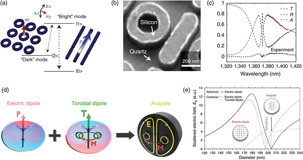
    Fig. 2. Fano resonances and AMs in dielectric nanostructures. (a) Schematic illustration of the interference between the bright- and the dark-mode resonators, (b) corresponding SEM image of a single-unit cell of the fabricated metasurface, and (c) corresponding experimental transmittance (T), reflectance (R), and absorption (A) spectra, showing a Fano-type resonance (Ref. 114). (d) Schematic illustration of an anapole excitation: the toroidal dipole moment is associated with the circulating magnetic field M accompanied by electric poloidal current distribution. As the symmetries of the radiation patterns of the electric P and toroidal T dipole modes are similar, they can destructively interfere, leading to total scattering cancelation in the far-field with nonzero near-field excitation (Ref. 115). (e) Calculated spherical electric dipole (black), Cartesian electric (red) and toroidal (green) dipole moments contribution to the scattering by a dielectric spherical particle of refractive index n=4 and wavelength 550 nm, as a function of the diameter. The anapole excitation is associated with the vanishing of the spherical electric dipole when the Cartesian electric and toroidal dipoles cancel each other (Ref. 115). Figure reprinted with permission: (a)–(c) Ref. 114, © 2014 by NPG; (d) and (e) Ref. 115, © 2015 by NPG.
    Third-order nonlinear effects. (a) THG spectroscopy of Si nanodisk arrays. The negative logarithm of the normalized transmission spectrum of the sample with period p=0.8 μm, height h=220 nm, and diameter d=0.5 μm is shown by the gray area, indicating a resonance at 1.24 μm. The THG spectrum of the sample (purple dots) shows a strong enhancement within the spectral band of the resonance. The inset shows the SEM image of the sample (Ref. 121). (b) Power dependence and conversion efficiency of the resonant THG process in Si nanodisks. Blue circles denote the THG power dependence obtained at λ=1.26 μm fundamental wavelength. Left inset: photographic image of the sample irradiated with the invisible IR beam. The blue point is the scattered THG signal. Right inset: conversion efficiency of the nanodisk sample as a function of the pump power (Ref. 121). (c) THG power as a function of the pump power for the Fano-resonance metasurface. The red circles indicate the measured data, and the blue line is a numerical fit to the data with a third-order power function. Left inset: SEM image of the sample; right inset: extracted absolute THG efficiency (Ref. 122). (d) Measured THG power versus the excitation of the AM in silicon nanodisks. Left inset: THG intensity image taken at λpump=1650 nm; scale bar is 1 μm and top view of the simulated distribution of the electric field intensity for a disk diameter of 875 nm. Right inset: conversion efficiency as a function of pump power (Ref. 127). (e) Measured nonlinear response of a Ge disk when exciting at HOM1 and HOM2 modes simultaneously. Inset: extinction spectrum of a Ge disk of 200-nm height and 625-nm radius (Ref. 129). (f) Measured nonlinear response of the Ge disk when exciting at two different wavelengths comprising HOM1 (Ref. 129). Figure reprinted with permission: (a) and (b) Ref. 121, © 2014 by the American Chemical Society (ACS); (c) Ref. 122, © 2015 by ACS; (d) Ref. 127, © 2016 by ACS; (e) and (f) Ref. 129, © 2017 by ACS.
    Fig. 3. Third-order nonlinear effects. (a) THG spectroscopy of Si nanodisk arrays. The negative logarithm of the normalized transmission spectrum of the sample with period p=0.8  μm, height h=220  nm, and diameter d=0.5  μm is shown by the gray area, indicating a resonance at 1.24  μm. The THG spectrum of the sample (purple dots) shows a strong enhancement within the spectral band of the resonance. The inset shows the SEM image of the sample (Ref. 121). (b) Power dependence and conversion efficiency of the resonant THG process in Si nanodisks. Blue circles denote the THG power dependence obtained at λ=1.26  μm fundamental wavelength. Left inset: photographic image of the sample irradiated with the invisible IR beam. The blue point is the scattered THG signal. Right inset: conversion efficiency of the nanodisk sample as a function of the pump power (Ref. 121). (c) THG power as a function of the pump power for the Fano-resonance metasurface. The red circles indicate the measured data, and the blue line is a numerical fit to the data with a third-order power function. Left inset: SEM image of the sample; right inset: extracted absolute THG efficiency (Ref. 122). (d) Measured THG power versus the excitation of the AM in silicon nanodisks. Left inset: THG intensity image taken at λpump=1650  nm; scale bar is 1  μm and top view of the simulated distribution of the electric field intensity for a disk diameter of 875 nm. Right inset: conversion efficiency as a function of pump power (Ref. 127). (e) Measured nonlinear response of a Ge disk when exciting at HOM1 and HOM2 modes simultaneously. Inset: extinction spectrum of a Ge disk of 200-nm height and 625-nm radius (Ref. 129). (f) Measured nonlinear response of the Ge disk when exciting at two different wavelengths comprising HOM1 (Ref. 129). Figure reprinted with permission: (a) and (b) Ref. 121, © 2014 by the American Chemical Society (ACS); (c) Ref. 122, © 2015 by ACS; (d) Ref. 127, © 2016 by ACS; (e) and (f) Ref. 129, © 2017 by ACS.
    Nonlinear phase control with silicon metasurfaces. (a) Geometries and nonlinear phases of Si nanopillar metaatoms. Shown are the sizes of the nanopillars and corresponding analytical and numerical results for the phase of the third-harmonic field for a pump wavelength of 1615 nm and linear polarization of the pump along the a-axis. (b) SEM image of the silicon metasurface. (c) Phase profile of the THG field encoded into the metasurface. (d) k-space image of the forward THG signal. A total of 92% of THG is directed into the designed diffraction angle θ=5.6 deg, where kx/k0=−0.098. (e) Cross section of a generated donut-shaped vortex beam at the THG taken along the propagation direction behind the metasurface. Inset: cross-section perpendicular to the optical axis at distance z=25 μm (Ref. 130). Figure reprinted with permission: (a)–(e) Ref. 130, © 2018 by ACS.
    Fig. 4. Nonlinear phase control with silicon metasurfaces. (a) Geometries and nonlinear phases of Si nanopillar metaatoms. Shown are the sizes of the nanopillars and corresponding analytical and numerical results for the phase of the third-harmonic field for a pump wavelength of 1615 nm and linear polarization of the pump along the a-axis. (b) SEM image of the silicon metasurface. (c) Phase profile of the THG field encoded into the metasurface. (d) k-space image of the forward THG signal. A total of 92% of THG is directed into the designed diffraction angle θ=5.6deg, where kx/k0=0.098. (e) Cross section of a generated donut-shaped vortex beam at the THG taken along the propagation direction behind the metasurface. Inset: cross-section perpendicular to the optical axis at distance z=25  μm (Ref. 130). Figure reprinted with permission: (a)–(e) Ref. 130, © 2018 by ACS.
    Second-order nonlinear effects at GaAs metasurfaces. (a) SHG power dependence at low pump intensities, and the deviation from the quadratic relationship at higher pump intensities due to the damage of GaAs resonators. Left inset: SEM image of the fabricated GaAs resonator array. Right inset: SHG conversion efficiency as a function of pump power (Ref. 132). (b) Schematic illustration of an optical metamixer consisting of a square array of subwavelength GaAs dielectric resonators. Two femtosecond near-IR pulses pump the metamixer and a variety of new frequencies are simultaneously generated. Top inset: SEM image of the GaAs metamixer (scale bar 3 μm). Bottom inset: energy diagrams of the seven nonlinear optical processes that occur simultaneously at the metasurface: SHG, THG, FHG, SFG, TPA-PL, FWM, and SWM (Ref. 133). (c) Measured nonlinear spectrum exhibiting 11 generated peaks originating from seven different nonlinear processes when two optical beams at λ2∼1.24 μm and λ1∼1.57 μm are used to simultaneously pump the GaAs metasurface. Blue labels indicate harmonic-generation processes and photoluminescence arising from two-photon absorption that each requires only one pump beam. Red labels indicate frequency mixing that involves both pump beams (Ref. 133). Figure reprinted with permission: (a) Ref. 132, © 2016 by ACS; (b) and (c) Ref. 133, © 2018 by NPG.
    Fig. 5. Second-order nonlinear effects at GaAs metasurfaces. (a) SHG power dependence at low pump intensities, and the deviation from the quadratic relationship at higher pump intensities due to the damage of GaAs resonators. Left inset: SEM image of the fabricated GaAs resonator array. Right inset: SHG conversion efficiency as a function of pump power (Ref. 132). (b) Schematic illustration of an optical metamixer consisting of a square array of subwavelength GaAs dielectric resonators. Two femtosecond near-IR pulses pump the metamixer and a variety of new frequencies are simultaneously generated. Top inset: SEM image of the GaAs metamixer (scale bar 3  μm). Bottom inset: energy diagrams of the seven nonlinear optical processes that occur simultaneously at the metasurface: SHG, THG, FHG, SFG, TPA-PL, FWM, and SWM (Ref. 133). (c) Measured nonlinear spectrum exhibiting 11 generated peaks originating from seven different nonlinear processes when two optical beams at λ21.24  μm and λ11.57  μm are used to simultaneously pump the GaAs metasurface. Blue labels indicate harmonic-generation processes and photoluminescence arising from two-photon absorption that each requires only one pump beam. Red labels indicate frequency mixing that involves both pump beams (Ref. 133). Figure reprinted with permission: (a) Ref. 132, © 2016 by ACS; (b) and (c) Ref. 133, © 2018 by NPG.
    Ultrafast optical switching with silicon metasurfaces. (a) Experimental (dots) and theoretical (solid lines) dependencies of the normalized reflectance change on the laser fluence (F) for three cases: (i) a 220-nm-thick silicon film (marked by black color), (ii) the “near-resonance nanoparticle” (marked by red color) and (iii) the “off-resonance nanoparticle” (marked by green color). Inset: schematic illustration of the scattering manipulation by an intense femtosecond laser pulse. The intense laser pulse switches the scattering of the particle to a Huygens source regime when the incident light is scattered in the forward direction (Ref. 154). (b) Left: illustration of the ultrafast all-optical switching in resonant silicon nanodisks based on two-photon absorption. Right: tailoring the all-optical switching in silicon nanodisks. Shown are the relative transmission changes for different samples (Ref. 155). Figure reprinted with permission: (a) Ref. 154, © 2015 by ACS; (b) Ref. 155, © 2015 by ACS.
    Fig. 6. Ultrafast optical switching with silicon metasurfaces. (a) Experimental (dots) and theoretical (solid lines) dependencies of the normalized reflectance change on the laser fluence (F) for three cases: (i) a 220-nm-thick silicon film (marked by black color), (ii) the “near-resonance nanoparticle” (marked by red color) and (iii) the “off-resonance nanoparticle” (marked by green color). Inset: schematic illustration of the scattering manipulation by an intense femtosecond laser pulse. The intense laser pulse switches the scattering of the particle to a Huygens source regime when the incident light is scattered in the forward direction (Ref. 154). (b) Left: illustration of the ultrafast all-optical switching in resonant silicon nanodisks based on two-photon absorption. Right: tailoring the all-optical switching in silicon nanodisks. Shown are the relative transmission changes for different samples (Ref. 155). Figure reprinted with permission: (a) Ref. 154, © 2015 by ACS; (b) Ref. 155, © 2015 by ACS.
    Basudeb Sain, Cedrik Meier, Thomas Zentgraf. Nonlinear optics in all-dielectric nanoantennas and metasurfaces: a review[J]. Advanced Photonics, 2019, 1(2): 024002
    Download Citation