
Shilei Jin, Longtao Xu, Peter Herczfeld, Ashish Bhardwaj, and Yifei Li, "Recent progress in attenuation counterpropagating optical phase-locked loops for high-dynamic-range radio frequency photonic links [Invited]," Photonics Res. 2, B45 (2014)
- Photonics Research
- Vol. 2, Issue 4, B45 (2014)
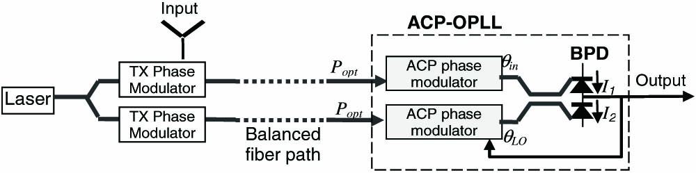
Fig. 1. PM RF/photonic link with an ACP-OPLL phase demodulator.
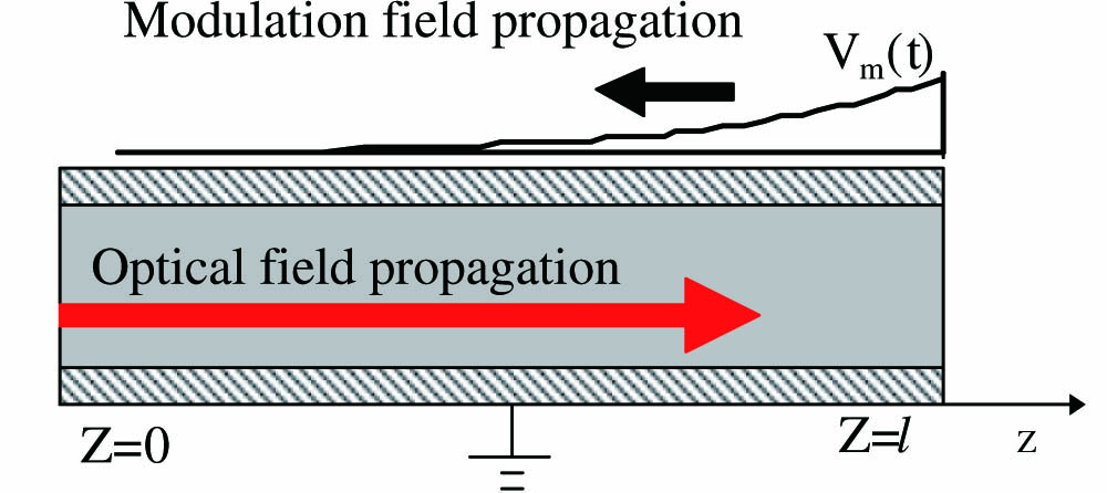
Fig. 2. ACP phase modulator.
Fig. 3. System model for a PM RF/photonic link.
Fig. 4. SFDR as a function of ϕ IP 3
Fig. 5. ACP-OPLL delay margin versus open loop gain and bandwidth.
Fig. 6. Schematic of a hybrid integrated ACP-OPLL.
Fig. 7. BPD of the hybrid ACP-OPLL.
Fig. 8. ACP-OPLL experiment setup.
Fig. 9. Measured ACP-OPLL OIP3 as a function of photocurrent.
Fig. 10. Output IMD: (a) output of an IM–direct detection (IM-DD) link with a MZ intensity modulator and (b) measured output spectrum of a hybrid ACP-OPLL in an identical modulation index condition.
Fig. 11. SFDR measurements: (a) 50 MHz; (b) 100 MHz; (c) 200 MHz; (d) 300 MHz.
Fig. 12. Schematic of a monolithically integrated ACP-OPLL.
Fig. 13. MQW phase modulator design.
Fig. 14. Push–pull ACP phase modulator pair: (a) top view of a modulator section and (b) modulator cross section.
Fig. 15. (a) HFSS model and (b) simulated RF reflection from the modulator connection stub.
Fig. 16. Phase modulator response. (a) Amplitude response and (b) phase response.
Fig. 17. Balanced counterpropagating waveguide photodetector pair.
Fig. 18. Optical field propagation inside a waveguide photodetector.
Fig. 19. Frequency response of the BPD voltage output (a) with 50 Ω load impedance, (b) with 300 Ω load impedance.
Fig. 20. Simulated performance of the 2 × 2
Fig. 21. ACP-OPLL PIC.
Fig. 22. Simulated SFDR of the ACP-OPLL PIC with 50 Ω photodetector load impedance.
Fig. 23. Simulated NF of the ACP-OPLL PIC with 50 Ω photodetector load impedance.
Fig. 24. ACP-OPLL phase margin versus photocurrent, assuming 50 Ω photodetector load impedance.
Fig. 25. Microscope image of ACP-OPLL PICs bonded on an AlN subcarrier.
Fig. 26. Two-tone RF input at 200 MHz: (a) output spectrum from the IM-DD link and (b) output spectrum of the ACP-OPLL.


Set citation alerts for the article
Please enter your email address

© Copyright 2018-2021 | Chinese Laser Press. All Rights Reserved 沪ICP备15018463号-20