Abstract
In order to achieve small size, light weight, and immunity to electromagnetic interference, it is desirable to replace bulky coaxial cables with optical fiber in advanced radar front-ends. Such applications require a large dynamic range that is beyond the reach of conventional intensity modulation–direct detection fiber-optic links. A coherent fiber-optic link employing an optical phase-locked loop (OPLL) phase demodulator has been proposed as a solution to this problem. The challenge is the practical realization of the OPLL demodulator that satisfies the stringent loop delay requirement. A novel attenuation counterpropagating (ACP) OPLL concept has been proposed and demonstrated as a solution. In this paper we review the recent progress in realizing chip-scale ACP-OPLL devices. In particular, we focus on the latest measurement results achieved using a hybrid integrated ACP-OPLL, as well as the design and performance potential of a monolithically integrated ACP-OPLL photonic integrated circuit.1. INTRODUCTION
Restricted front-end spurious free dynamic range (SFDR) is a common limiting factor in many radar receivers [1–7]. Conventional electronic receiver front-ends rely on transistors and diodes for signal amplification and frequency mixing. Both transistors and diodes contain inherent nonlinearities, resulting in limited SFDR. On the other hand, photonic radar front-ends employ RF/photonics links. Prevalent RF/photonic links employ intensity modulation (IM) schemes that are nonlinear and thus also restrict the dynamic range. Various linearization methods, such as predistortion and postdistortion linearizers, have been explored for improving the SFDR of electronic amplifiers and mixers [1–3]. However, the SFDR enhancement is small, and the bandwidth is narrow in these cases. Linearizers have also been applied to RF/photonic links with similar results [4–7].
To solve the problem of limited SFDR, a linear phase-modulated RF/photonic link with an optical phase-locked loop (OPLL) phase demodulator (see Fig. 1) has been proposed [8,9]. It relies on the notion that optical phase modulation (PM) can be highly linear. Thus, using a linear phase demodulator, a high-dynamic-range RF/photonic link can be realized. The most critical part of the link is the OPLL linear phase demodulator. The OPLL demodulates the optical phase by tight phase tracking. It must have a large open loop gain over a wide bandwidth. For feedback stability, the OPLL only tolerates very short loop propagation delay [8]. This delay requirement can be met by employing an OPLL concept with attenuating counterpropagating (ACP) optical and RF fields [10]. Chip-scale ACP-OPLL devices have been implemented using both hybrid [8] as well as monolithic integration [11]. It is to be noted that hybrid integration refers to a device, where different components of a device can be designed on different chips, whereas monolithic integration refers to a device where all of its components are monolithically integrated onto a single chip. Hybrid integration is advantageous as it enables the use of suitable materials for realizing the internal components of the OPLL. On the other hand, monolithic integration allows for shorter loop propagation delay and consequently a larger ACP-OPLL bandwidth than what can be achieved using hybrid integration. Monolithic integration has the potential to improve the ACP-OPLL’s power and cost efficiencies. In this paper we review the recent progress in developing integrated ACP-OPLLs. We put emphasis on the new experimental results obtained from a hybrid integrated ACP-OPLL as well as the design and performance that can be achieved using a monolithically integrated ACP-OPLL. Both of these topics have not been discussed in previous publications.
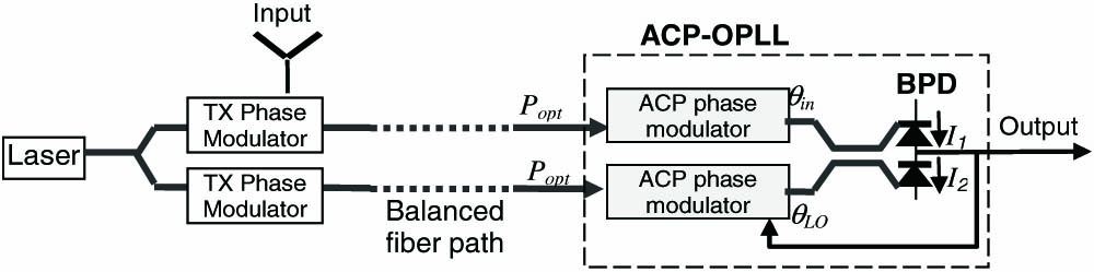
Figure 1.PM RF/photonic link with an ACP-OPLL phase demodulator.
2. ATTENUATION COUNTERPROPAGATING OPTICAL PHASE-LOCKED LOOP CONCEPT
As shown in Fig. 1, an ACP-OPLL contains an ACP phase modulator pair, a compact 3 dB coupler, and a high-power-balanced photodetector (BPD) pair. The key here is the ACP phase modulator (see Fig. 2). In the ACP phase modulator, the optical field and the modulation RF field counterpropagate, and the RF field experiences strong attenuation. The modulator propagation delay is thereby eliminated, and consequently the OPLL feedback stability is improved. Through the feedback, the ACP-OPLL demodulates the incoming differential optical phase by tightly tracking the optical phase. The theoretical performance of a PM optical link employing the ACP-OPLL was studied using a system model [8] shown in Fig. 3. In Fig. 3, is the optical power of each optical path entering the OPLL, represents the incoming differential phase that carries information, is the responsivity of the photodiode, is the termination impedance of the photodiode, and are the PM sensitivities of the transmitter (TX) and the ACP phase modulator pair, respectively, and is the propagation delay due to the 3 dB coupler and the feedback path. The phase delays for the photodetector and the local phase modulator are included in and , respectively. is the shot noise of the BPD: where is the charge of a single electron and is the DC photocurrent of each photodetector; that is, .
Sign up for Photonics Research TOC. Get the latest issue of Photonics Research delivered right to you!Sign up now

Figure 2.ACP phase modulator.
Figure 3.System model for a PM RF/photonic link.
Using Fig. 3, we first determine the link gain in the small signal condition () to be where is the ACP-OPLL open loop gain, given by Also from Fig. 3, we determine the link noise figure (NF) in the photodetector shot noise limit to be where is the termination impedance of the transmitter phase modulator electrode, is the Boltzmann constant, and is the environmental temperature.
The link SFDR in the photodetector shot noise limit is given by where is the demodulation phase third-order intercept point (IP3) of the ACP-OPLL, given by where is the demodulation phase IP3 set by the OPLL internal homodyne phase demodulation mechanism, and is the phase IP3 of the ACP phase modulator set by the modulator nonlinearity. They are given by where is the length of the ACP phase modulator, and is modulator phase IP3 per unit length. is determined through measurements.
As shown in Fig. 4, in order to achieve a SFDR over , should be larger than assuming 50 mA of photocurrent per detector. Over 50 mA of photocurrent is a reasonable expectation for high-power unitraveling carrier (UTC) photodetectors prior to saturation [12,13]. This requirement necessitates an open loop gain of 20 dB or larger. To ensure feedback stability in presence of a large open loop gain over a wide bandwidth, the ACP-OPLL can only tolerate very small loop propagation delay (see Fig. 5). Minimizing the loop delay is one of the most critical tasks for realizing the ACP-OPLL.
Figure 4.SFDR as a function of and the photocurrent per photodetector.
Figure 5.ACP-OPLL delay margin versus open loop gain and bandwidth.
3. HYBRID INTEGRATED ATTENUATION COUNTERPROPAGATING OPTICAL PHASE-LOCKED LOOPS
Hybrid integration enables the loop components of the OPLL to be realized using the most suitable material systems and obtain superior optical performance for each optical functionality. In the current version of the hybrid integrated ACP-OPLL, as shown in Fig. 6, the ACP local phase modulator and the 3 dB coupler of the hybrid integrated ACP-OPLL are realized on a chip. is a suitable material to realize linear, low-loss optical phase modulators. The ACP phase modulator is designed to be 6.8 cm long. To achieve the desired attenuation of the RF modulation signal, the modulator employs a thin film electrode with a 100 Å Ti layer and a 1000 Å Au layer. The phase modulator has a measured of . The ACP-OPLL employs a conventional coupled-line 3 dB coupler. To minimize the delay, the output of the coupler is directly butt-coupled to a pair of UTC BPDs. Different from the previously reported hybrid ACP-OPLL [8], the ACP-OPLL in this paper contains a pair of back-illuminated UTC photodetectors. They sit on an AlN submount (see Fig. 7). This new BPD pair has improved responsivity and saturation optical power.
Figure 6.Schematic of a hybrid integrated ACP-OPLL.
Figure 7.BPD of the hybrid ACP-OPLL.
The ACP-OPLL was characterized using the setup shown in Fig. 8. The laser source is a 1550 nm single-frequency narrow-linewidth fiber laser (Orbits ETH-20-1550). Its output is amplified using an erbium-doped fiber amplifier (EDFA). In order to reduce the noise due to amplified spontaneous emission, the output of the EDFA is filtered by a narrow-band () fiber Bragg grating (FBG). Then the light is split into two paths using a 3 dB optical coupler. One path contains a Tx optical phase modulator, which accepts the RF input. The other path contains the ACP optical phase modulator of the ACP-OPLL. The two paths are recombined using another 3 dB coupler and then are butt-coupled to the BPD pair. The output of the ACP-OPLL is extracted by a ground-signal-ground (GSG) probe through a 70 Ω resistor. Standard two-tone intermodulation tests were performed to evaluate the phase demodulation linearity (or OIP3) of the ACP-OPLL.
Figure 8.ACP-OPLL experiment setup.
As shown in Fig. 9, initially the measured ACP-OPLL OIP3 was improved when increasing the photodetector current (or the input optical power). This is expected as larger photocurrent results in larger open loop gain, and consequently better OPLL phase demodulation linearity (see Eq. (7)). However, when the photocurrent was raised above 60 mA, the OIP3 started to decrease. We attribute this behavior to the nonlinearity of the photodetector. Figure 10(b) shows a sample of the ACP-OPLL output captured by a microwave spectrum analyzer. The RF input is 10 dBm per tone, centered at 103 MHz, and the photocurrent is 60 mA per photodetector. The measured third-order intermodulation distortion (IMD3) is . This is 60 dB better than the distortion of a conventional Mach–Zehnder (MZ) modulator under an identical modulation condition [see Fig. 10(a)].
Figure 9.Measured ACP-OPLL OIP3 as a function of photocurrent.
Figure 10.Output IMD: (a) output of an IM–direct detection (IM-DD) link with a MZ intensity modulator and (b) measured output spectrum of a hybrid ACP-OPLL in an identical modulation index condition.
The output noise floor of the ACP-OPLL was measured after being amplified by 44 dB using two RF low-noise amplifiers (LNAs) (Mini Circuits ZX60-33LN+, 1 dB NF). From the noise floor and two-tone distortion measurements, the SFDR was determined. The results are summarized in Fig. 11. With 60 mA photocurrent per photodetector, the hybrid ACP-OPLL demonstrated SFDR at 50 MHz, SFDR at 100 MHz, SFDR at 200 MHz, and SFDR at 300 MHz. These represent the best measured SFDR values in a fiber-optic link. In addition, the measured noise floor is still higher than the theoretical value that is determined by the photodetector shot noise. This suggests that the ACP-OPLL output noise is dominated by the residual laser relative intensity noise (RIN) due to the imperfect balancing of the photodetector pair. The SFDR should improve further by improving the balancing of the photodetector pair.
Figure 11.SFDR measurements: (a) 50 MHz; (b) 100 MHz; (c) 200 MHz; (d) 300 MHz.
4. MONOLITHIC INTEGRATED ATTENUATION COUNTERPROPAGATING OPTICAL PHASE-LOCKED LOOPS
In order to shorten the loop delay and improve the power and cost efficiencies, monolithic integration of ACP-OPLL on an InP-based material platform was investigated [11].
A. Attenuation Counterpropagating Optical Phase-Locked Loops Design
A schematic of the monolithically integrated ACP-OPLL is shown in Fig. 12. It contains a pair of integrated InGaAsP multiquantum-well (MQW) phase modulators, a compact multimode interference (MMI) coupler, and a UTC waveguide photodetector. All OPLL components share a common quantum well optical waveguiding layer. Due to tighter integration and more efficient MQW phase modulator, a monolithically integrated ACP-OPLL should achieve higher operation frequency () than that of a hybrid interested ACP-OPLL ( of MHz).
Figure 12.Schematic of a monolithically integrated ACP-OPLL.
1. Push–Pull Balanced Attenuation Counterpropagating Phase Modulator
The main disadvantage of the InP material platform is the MQW phase modulator. Compared with the conventional phase modulators, the MQW phase modulator has a large optical propagation loss, parasitic IM, and nonlinearity. To mitigate these problems, we have developed a detuned shallow MQW modulator [14], which consists of 25 periods of lattice matched 9 nm thick quantum wells and 6.5 nm thick barriers as shown in Fig 13. To reduce the optical propagation loss and parasitic IM, the quantum well photoluminescence peak is set away from the 1.55 μm operating wavelength. The low quantum well barrier height reduces the quantum confinement at high bias voltages. This helps to create a linear PM region near a certain bias (). Using a 1 mm long shallow MQW phase modulator, phase IP3 of , optical propagation loss of (), and of were demonstrated. The linearity of a 3 mm long device in a balanced pair should have a combined phase IP3 of . This is sufficient to support an ACP-OPLL with SFDR larger than as shown in Fig. 4.
Figure 13.MQW phase modulator design.
However, the shallow MQW phase modulator still generates significant photocurrent for high optical input power, which presents a problem when implementing the ACP phase modulator as part of the OPLL. This is because the ACP modulator uses a lossy electrode with a large sheet resistance. If the photocurrent flows through the electrode, a significant voltage drop may be generated, resulting in a large bias voltage deviation from the optimum bias voltage (). To solve this problem, we conceived a push–pull balanced ACP modulator configuration as shown in Fig. 14.
Figure 14.Push–pull ACP phase modulator pair: (a) top view of a modulator section and (b) modulator cross section.
In Fig. 14, the left modulator has a lossy N-metal contact (electrode), and the right modulator has a lossy P-metal contact (electrode). The layer structures of the lossy N and P contacts are given by Ni–AuGe–Ni–Au (500–800–200–1200 Å) and Ti–Pt–Au (200–400–800 Å), respectively. Both metal contacts have a sheet resistance of . The two electrodes are connected by an array of metal stubs (10 μm wide). The separation between the adjacent stubs is 200 μm. The two phase modulators in Fig. 14 should generate complementing photocurrents. These photocurrents flow to the DC power supply though the metal stubs. No net photocurrent flow occurs on the lossy electrodes. Therefore, the optimum bias voltage is maintained along the modulator electrodes.
On the other hand, the connection stubs add discontinuity to the ACP-modulator electrode and consequently introduce reflection to the modulation signal on the electrode. Their impact to the performance of the push–pull ACP modulator was carefully studied. First, the reflection caused by a single stub was simulated using Ansoft HFSS, and the result is shown in Fig. 15. Below 20 GHz, the reflection is small, but it increases at higher frequency. Then, we simulated the frequency response of a 3 mm long ACP push–pull modulator pair with and without the reflection from these stubs. The 3 mm long ACP push–pull modulator pair contains 15 connection stubs. As shown in Fig. 16, the ACP modulator pair has a of and a 3 dB bandwidth of 1.15 GHz. In the phase response [Fig. 16(b)] the impact of the connection stubs is observed only when the frequency is larger than 200 GHz. This is 170 times larger than the modulator bandwidth. Thus, we conclude that the connection stubs should not cause any penalty in the phase margin of the ACP-OPLL.
Figure 15.(a) HFSS model and (b) simulated RF reflection from the modulator connection stub.
Figure 16.Phase modulator response. (a) Amplitude response and (b) phase response.
2. Balanced Counterpropagating Waveguide Unitraveling Carrier Photodetector
The layers that define the UTC-waveguide photodetector for the monolithic integrated ACP-OPLL are developed by Klamkin et al. [12], and are grown on top of the MWQ optical waveguide as shown in Fig. 12. The design of the BPD pair is shown in Fig. 17. To reduce its latency, the photodetector employs counterpropagating optical and RF fields [15]. The width and the length of the photodetector are 10 and 200 μm, respectively. The overlap between the absorbing layers of the detector and the optical mode is set to 1.4%. The detector absorption length (with 95% absorption) is (see Fig. 18). Figure 19 shows the frequency response of the photodetector output voltage when it is connected to the ACP phase modulator pair. The response depends on the photodetector’s load impedance. Its 3 dB bandwidth is with conventional 50 Ω load impedance. If the load impedance is raised to 300 Ω, the bandwidth is reduced to . However, the higher load impedance generates larger amplitude response. This helps to increase the OPLL open loop gain.
Figure 17.Balanced counterpropagating waveguide photodetector pair.
Figure 18.Optical field propagation inside a waveguide photodetector.
Figure 19.Frequency response of the BPD voltage output (a) with 50 Ω load impedance, (b) with 300 Ω load impedance.
3. Compact 2×2 Multimode Interference Coupler
The monolithic integrated ACP-OPLL uses a regular MMI coupler (see Fig. 20). The length of the coupler is 217 μm. The MMI coupler sets the total OPLL loop delay to be , which includes propagation delays of the MMI coupler, waveguide bends, tapers, and the feedback electrode.
Figure 20.Simulated performance of the MMI 3 dB coupler (217 μm long and 7 μm wide).
B. Performance Projection
The layout of a complete monolithic integrated ACP-OPLL photonic integrated circuit (PIC) is depicted in Fig. 21. The projected SFDR and NF performance in the photodetector shot noise limit were simulated, and the results are summarized in Figs. 22 and 23, respectively. In this simulation the BPD of the ACP-OPLL has conventional 50 Ω output load impedance, and the link transmitter phase modulator has a of 1 V. The projected SFDR scales with the photocurrent. When the photocurrent reaches 60 mA per photodetector, the ACP-OPLL PIC should achieve SFDR over 1 GHz bandwidth. In this scenario, the link NF should reach 4 dB. Figure 24 depicts stable phase margin of the ACP-OPLL as a function of the photocurrent. Even with 80 mA photocurrent, which represents a 22.9 dB open loop gain, the ACP-OPLL still has a phase margin greater than 40°.
Figure 21.ACP-OPLL PIC.
Figure 22.Simulated SFDR of the ACP-OPLL PIC with 50 Ω photodetector load impedance.
Figure 23.Simulated NF of the ACP-OPLL PIC with 50 Ω photodetector load impedance.
Figure 24.ACP-OPLL phase margin versus photocurrent, assuming 50 Ω photodetector load impedance.
C. Measurement of the Monolithically Integrated Attenuation Counterpropagating Optical Phase-Locked Loops
The fabricated ACP-OPLL PIC is shown in Fig. 25. Details on the device fabrication and measurement were discussed in [16] and [11], respectively. It was found that the UTC waveguide photodetectors on the fully fabricated ACP-OPLL PICs demonstrated smaller responsivity and narrower bandwidth compared to what could be expected from these devices (see Fig. 19). Only 15 mA photocurrent was generated in each photodetector of the ACP-OPLL PIC, which limited the performance of the ACP-OPLL PIC. Figure 26 shows the output of the ACP-OPLL PIC in a two-tone intermodulation test at 200 MHz. The distortion is 39 dB better than that of a conventional MZ modulator under a similar modulation index condition. The measured SFDR of the ACP-OPLL PIC is over 300 MHz as reported in [11].
Figure 25.Microscope image of ACP-OPLL PICs bonded on an AlN subcarrier.
Figure 26.Two-tone RF input at 200 MHz: (a) output spectrum from the IM-DD link and (b) output spectrum of the ACP-OPLL.
5. CONCLUSION
In this paper we have reviewed the recent progress in developing the ACP-OPLL for high-dynamic-range RF/photonic links. We focused on two types of ACP-OPLL devices: the hybrid integrated ACP-OPLL and the monolithically integrated ACP-OPLL.
For hybrid integration, each ACP-OPLL loop component is realized using the most suitable material system. In particular is used to implement the ACP local phase modulator. The ACP phase modulator is a linear phase modulator free of unwanted nonlinearity and electroabsorption. Using an improved backside illuminated UTC photodetector, the new hybrid ACP-OPLL device demonstrated SFDR at 50 MHz, SFDR at 100 MHz, SFDR at 200 MHz, and SFDR at 300 MHz. To the best of our knowledge, these values represent the highest SFDR that has been demonstrated in a RF/photonic link.
On the other hand, a monolithically integrated ACP-OPLL can achieve short loop delay, large bandwidth, and superior power and cost efficiencies compared with the hybrid integrated ACP-OPLL. An InP-based material platform is used for monolithic integration. The main disadvantage of this material platform is the integrated InP MQW phase modulator, which is nonlinear, lossy, and contains parasitic IM. A push–pull shallow MQW ACP phase modulator pair was developed to mitigate these problems. The design and potential performance of the monolithic integrated ACP-OPLL were discussed in detail. Simulation results showed that a monolithically integrated ACP-OPLL is capable of achieving SFDR over 1 GHz.
A monolithically integrated ACP-OPLL PIC has been fabricated. The BPDs of the ACP-OPLL PIC demonstrated smaller responsivity and narrower bandwidth than what could be expected from these devices. Consequently, the SFDR of the ACP-OPLL was limited to in 300 MHz bandwidth. The current efforts focus on modifying the fabrication process to increase the photodetector responsivity and bandwidth in order to achieve the full performance potential that can be obtained from a monolithically integrated ACP-OPLL.
References
[1] S.-Y. Lee, L. Yong-Sub, H. Seung-Ho, H.-S. Choi, J. Yoon-Ha. Independently controllable 3rd- and 5th-order analog predistortion linearizer for RF power amplifier in GSM. Proceedings of IEEE Asia-Pacific Conference on Advanced System Integrated Circuits, 146-149(2004).
[2] J.-H. Han, D.-H. Lee, N. Sangwook, L. Jong-Sik, Y. Jongsup, K. Sungchoon. Post-distortion linearizer for multicarrier power amplifiers using a fifth-order error signal generator. Proceedings of 2001 Asia–Pacific Microwave Conference, 272-275(2001).
[3] C. Kyoung-Joon, K. Wan-Jong, K. Jong-Heon, S. P. Stapleton. Linearity optimization of a high power Doherty amplifier based on post-distortion compensation. IEEE Microw. Wireless Compon. Lett., 15, 748-750(2005).
[4] J. H. Schaffner, W. B. Bridges. Intermodulation distortion in high dynamic range microwave fiber-optic links with linearized modulators. J. Lightwave Technol., 11, 3-6(1993).
[5] Y. Chiu, B. Jalali, S. Garner, W. Steier. Broad-band electronic linearizer for externally modulated analog fiber-optic links. IEEE Photon. Technol. Lett., 11, 48-50(1999).
[6] E. I. Ackerman, C. H. Cox. Effect of pilot tone-based modulator bias control on external modulation link performance. Proceedings of International Topical Meeting on Microwave Photonics, 121-124(2000).
[7] G. Betts. Linearized modulator for suboctave-bandpass optical analog links. IEEE Trans. Microwave Theor. Tech., 42, 2642-2649(1994).
[8] Y. Li, P. Herczfeld. Coherent PM optical link employing ACP-PPLL. J. Lightwave Technol., 27, 1086-1094(2009).
[9] J. Klamkin, L. A. Johansson, A. Ramaswamy, J. E. Bowers, S. P. DenBaars, L. A. Coldren. Monolithically integrated coherent receiver for highly linear microwave photonic links. Proceedings of the 20th Annual Meeting of the IEEE Lasers and Electro-Optics Society, 40-41(2007).
[10] Y. Li, P. R. Herezfeld. Novel attenuation-counter-propagating phase modulator for highly linear fiber-optic links. J. Lightwave Technol., 24, 3709-3718(2006).
[11] Y. Li, A. Bhardwaj, R. Wang, S. Jin, L. Coldren, J. Bowers, P. Herczfeld. A monolithically integrated ACP-OPLL receiver for RF/photonic links. IEEE Photon. Technol. Lett., 23, 1475-1477(2011).
[12] J. Klamkin, C. Yu-Chia, A. Ramaswamy, L. A. Johansson, J. E. Bowers, S. P. DenBaars, L. A. Coldren. Output saturation and linearity of waveguide unitraveling-carrier photodiodes. IEEE J. Quantum Electron., 44, 354-359(2008).
[13] X. Li, N. Li, X. Zheng, S. Demiguel, J. Campbell, D. Tulchinsky, K. Williams. High-speed high-saturation-current InP/In0.53Ga0.47As photodiode with partially depleted absorber. Optical Fiber Communications Conference, 338-339(2003).
[14] Y. Li, W. Renyuan, A. Bhardwaj, S. Ristic, J. Bowers. High linearity InP-Based phase modulators using a shallow quantum-well design. IEEE Photon. Technol. Lett., 22, 1340-1342(2010).
[15] Y. Li, W. Renyuan, J. Klamkin, S. M. Madison, P. W. Juodawlkis, P. Herczfeld, J. E. Bowers. Propagation delay of waveguide photodetector. J. Lightwave Technol., 28, 2099-2104(2010).
[16] A. Bhardwaj, Y. Li, R. Wang, S. Jin, P. Herczfeld, J. E. Bowers, L. A. Coldren. Monolithic integration of high linearity attenuated counter-propagating optical phase-locked loop coherent receiver. Electron. Lett., 47, 1090-1092(2011).


