
Jinjing Huang, Jun Liu. A complete small-signal HBT model including AC current crowding effect[J]. Journal of Semiconductors, 2021, 42(5): 052401
- Journal of Semiconductors
- Vol. 42, Issue 5, 052401 (2021)
Abstract
1. Introduction
Heterojunction bipolar transistors (HBTs) have been extensively used in high-speed analog, digital and mixed-signal integrated circuits (ICs)[
However, most of the reported topologies ignore the AC current crowding effect[
In recent years, different small-signal equivalent circuits have been proposed with various extraction methods, in which π[
2. Small-signal model
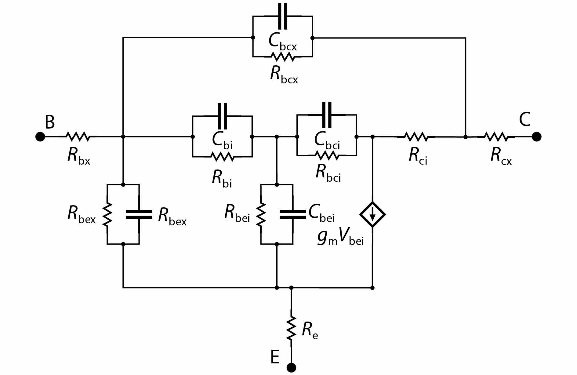
The complete small-signal equivalent circuit of the HBT device considering the AC current crowding effect is given in Fig. 1.
![]()
Figure 1.Complete small-signal equivalent circuit of HBT device including
In Fig. 1, Rbx, Rcx, Re are the base, collector, and emitter parasitic resistances, respectively. Rbcx and Rbex are the extrinsic base-collector and base-emitter resistances, and Cbcx and Cbex are the extrinsic base-collector and base-emitter depletion capacitances. Rbi and Rci are the intrinsic resistances, and Cbi is the intrinsic base capacitance. The parallel RC circuit composed of Cbi and Rbi characterizes the AC current crowding effect. Rbci, Rbei, Cbci and Cbei are the intrinsic resistances and capacitances, respectively. gm and gm0 are the small-signal and DC transconductances, respectively. τ is the delay time.
Circuit topology demonstrated in Fig. 1 can be simplified to facilitate calculation. We introduce three parameters, Arbe, Arc and Abex with a value range of (0, 1) and stipulate
3. Extraction procedure
3.1. Parasitic resistances
Since the parasitic resistances Rbx, Rc and Re are independent of the bias condition, we extract them under zero biasing conditions in this work. The calculation equations are given as follows[
Through Y–Z transformation, Ym can also be expressed as
where
3.2. Intrinsic part parameters
Once the parasitic resistances are known, the extraction of the intrinsic parameters can be carried out[
![]()
Figure 2.Small-signal equivalent circuit after de-embedding the extrinsic parameters.
The circuit in Fig. 2 can be converted to that in Fig. 3 after T-π transformation[
![]()
Figure 3.Final circuit after T-π transformation.
Combining Eqs. (6)–(9), Yin can also be represented by Z1, Z2, Z3, and Z4, which are expressed as[
in which
Then, we can get that
Based on the above relationship between Yin and Z1, Z2, Z3, the extraction method reported in Ref. [18] is used to extract the parameters. From Eqs. (13) and (14), we can get
Defining
where
Since Z1 and Z3 are given in Eqs. (13) and (14), the ω2 dependence of F0 can be easily plotted in Fig. 4. Then A0 and B0 can be determined. Tbi is defined as
![]()
Figure 4.Frequency of
Based on Eq. (7), Z1 can be written as
where
Defining
where
A1 and B1 can be obtained by using the straight-line fitting method. Then, Tbe can be determined as
Based on Eqs. (22) and (25), we can get
By extracting the real and imaginary parts of F2, Rx and Tx can be acquired from Eqs. (30) and (31).
Based on Eqs. (23) and (24), the expressions of Rx and RxTx can be written as
Rbe, Rbi can be determined from Eqs. (17), (18), (20), (28), (30), and (31). When Rbe and Rbi are obtained, Rbc, Cbc, Cbe and Cbi can be obtained from Eqs. (17), (18), (25), and (26), respectively.
In the end, the remaining parameters are written as
4. Model verification
An GaAs HBT with 2 μm emitter linewidth was used to validate the accuracy of the equivalent circuit. The adopted device was manufactured in a commercial foundry. The method in Section 3 is applied to extract the parameters of an HBT device with a 2 × 20 μm2 emitter-area under bias points of Bias1 (Vce = 1 V, Ib = 15 μA), Bias2 (Vce = 1 V, Ib = 30 μA) and Bias3 (Vce = 3 V, Ib = 17.5 μA) in the frequency range from 100 MHz to 20 GHz. After extracting all parameters, the Keysight ICCAP software is used to optimize the extracted parameters to further reduce the error between the simulated and measured data. Here, the initial values of Arbe, Arc and Abex are set to 0.5 for optimization. Results of the extraction are compared with the extracted from the small-signal equivalent circuit of an AHBT (agilent heterojunction bipolar transistor) without considering Cbi. Table 1 shows the initial extraction and optimization results of the HBT device under Bias1 and Bias3. The comparisons of the real part and the imaginary part between the simulated and measured S-parameters are plotted in Fig. 5. The accuracy of S-parameters versus frequency shows in Table 2.
![]()
Figure 5.
Due to the inaccurate initial value of 0.5 for the partition parameters Arc, Arbe, and Abex defined before extraction, the extracted and optimized values of Rcx, Rci, Rbcx, Rbex, Cbcx and Cbex are slightly larger. From Fig. 6, it can be seen that the proposed model with Cbi shows more accuracy than the one without Cbi, which verifies the effectiveness of the introduced AC current crowding effect.
![]()
Figure 6.(a) Plot of
Fig. 6 shows the decrease of Cbi with Ib and Vce. Results present that Cbi decreases with increasing Ib and Vce, which is consistent with the result shown in Ref. [18]. The experimental results show that the dependence between Cbi and biases accords with the basic capacitance equation.
5. Conclusion
An improved small-signal equivalent circuit of the HBT device considering the AC current crowding effect is proposed in this paper. This effect is modeled as a parallel RC circuit with Cbi and Rbi. By comparing between the simulated and measured S-parameters under three different biases, the results validate the reliability and availability of the proposed model and the developed extraction method.
Acknowledgements
This work was supported by the National Natural Science Foundation of China (Grant No. 61934006)
References
[1] J Zhang, M Liu, J Wang et al. Modeling of InP HBTs with an improved keysight HBT model. Microw J, 62, 56(2019).
[2] T Shivan, N Weimann, M Hossain et al. A highly efficient ultrawideband traveling-wave amplifier in InP DHBT technology. IEEE Microw Wirel Compon Lett, 28, 1029(2018).
[3] Z Griffith, M Urteaga, P Rowell. A 190-GHz high-gain, 3-dBm OP1dB low DC-power amplifier in 250-nm InP HBT. IEEE Microw Wirel Compon Lett, 27, 1128(2017).
[4]
[5] S C Huang, W B Tang, Y M Hsin. High-frequency noise modeling of InGaP/GaAs HBT with base-contact capacitance and AC current crowding effect. IEEE Electron Device Lett, 30, 1125(2009).
[6] S Yadav, A Chakravorty, M Schroter. Modeling of the lateral emitter-current crowding effect in SiGe HBTs. IEEE Trans Electron Devices, 63, 4160(2016).
[7] C Yapei, Z Yong, X Yuehang et al. Investigation of terahertz 3D EM simulation on device modeling and a new InP HBT dispersive inter-electrode impedance extraction method. IEEE Access, 6, 45772(2018).
[8] et al. Small-signal characterization and modelling of 55 nm SiGe BiCMOS HBT up to 325 GHz. Solid State Electron, 129, 150(2017).
[9] Y Sun, J Fu, Y Wang et al. Direct analytical parameter extraction for SiGe HBTs T-topology small-signal equivalent circuit. Superlattices Microstruct, 94, 223(2016).
[10] H S Rhee, S Lee, B R Kim. D. c. and a. c. current crowding effects model analysis in bipolar junction transistors using a new extraction method. Solid-State Electron, 38, 31(1995).
[11] W B Tang, C M Wang, Y M Hsin. A new extraction technique for the complete small-signal equivalent-circuit model of InGaP/GaAs HBT including base contact impedance and AC current crowding effect. IEEE Trans Microw Theory Tech, 54, 3641(2006).
[12] K Lee, K Choi, S H Kook et al. Direct parameter extraction of SiGeHBTs for the VBIC bipolar compact model. IEEE Trans Electron Devices, 52, 375(2005).
[13] D Dousset, A Issaoun, F M Ghannouchi et al. Wideband closed-form expressions for direct extraction of HBT small-signal parameters for all amplifier bias classes. IEEE Proceedings - Circuits, Devices and Systems, 152, 441(2005).
[14] T K Johansen, R Leblanc, J Poulain et al. Direct extraction of InP/GaAsSb/InP DHBT equivalent-circuit elements from S-parameters measured at cut-off and normal bias conditions. IEEE Trans Microw Theory Tech, 64, 115(2016).
[15] J C Zhang, B Liu, L M Zhang et al. A rigorous peeling algorithm for diret parameter extraction procedure of HBT small-signal equivalent circuit. Analog Integr Circuits Signal Process, 85, 405(2015).
[16] S Bousnina, P Mandeville, A B Kouki et al. Direct parameter-extraction method for HBT small-signal model. IEEE Trans Microw Theory Tech, 50, 529(2002).
[17] L Degachi, F M Ghannouchi. Systematic and rigorous extraction method of HBT small-signal model parameters. IEEE Trans Microw Theory Tech, 54, 682(2006).
[18] L Degachi, F M Ghannouchi. An augmented small-signal HBT model with its analytical based parameter extraction technique. IEEE Trans Electron Devices, 55, 968(2008).
[19] W Zhou, L Sun, J Liu et al. Extraction and verification of the small-signal model for InP DHBTs in the 0.2–325 GHz frequency range. ICE Electron Express, 15, 20180244(2018).
[20] A Zhang, J Gao, H Wang. Direct parameter extraction method for InP heterojunction bipolar transistors based on the combination of T- and π-models up to 110 GHz. Semicond Sci Technol, 35, 025001(2019).
[21] A Zhang, J Gao. A direct extraction method to determine the extrinsic resistances for InP HBT device based on S-parameters measurement up to 110 GHz. Semicond Sci Technol, 35, 075025(2020).

Set citation alerts for the article
Please enter your email address
© Copyright 2018-2021 | Chinese Laser Press. All Rights Reserved 沪ICP备15018463号-20