• Journal of Infrared and Millimeter Waves
  • Vol. 39, Issue 3, 306 (2020)
Kai-Juan ZHANG1, Chun-Qi SHI1,2, and Run-Xi ZHANG1,*
Author Affiliations
  • 1Institute of Microelectronic Circuits and Systems, East China Normal University, Shanghai20024, China
  • 2Key Laboratory of Multidimensional Information Processing, East China Normal University, Shanghai0041, China
  • show less
    DOI: 10.11972/j.issn.1001-9014.2020.03.007 Cite this Article
    Kai-Juan ZHANG, Chun-Qi SHI, Run-Xi ZHANG. A 94 GHz CMOS LNA utilizing dual-coupling gm-boosting technique[J]. Journal of Infrared and Millimeter Waves, 2020, 39(3): 306 Copy Citation Text show less
    The schematic of LNA and the 3D-view of passive devices
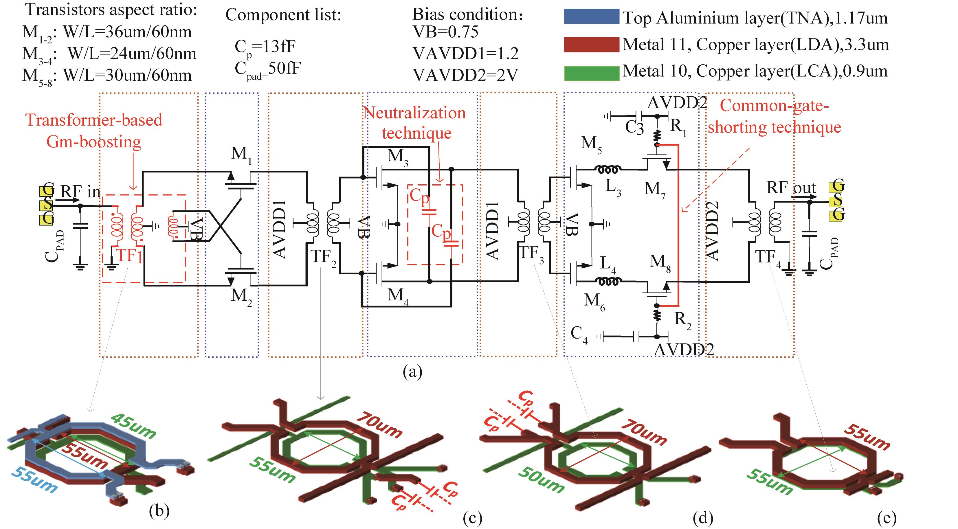
    Fig. 1. The schematic of LNA and the 3D-view of passive devices
    (a) The schematic of the dual-coupling gm-boosting technique; (b)the equivalent of the balun; (c) the equivalent half-circuit model of conventional source inductive degeneration; and (d) the equivalent half-circuit model of the dual-coupling gm-boosting technique
    Fig. 2. (a) The schematic of the dual-coupling gm-boosting technique; (b)the equivalent of the balun; (c) the equivalent half-circuit model of conventional source inductive degeneration; and (d) the equivalent half-circuit model of the dual-coupling gm-boosting technique
    Comparison of simulated Gmax for circuits which use the traditional source inductive degeneration (TSID) method and the dual-coupling gm-boosting (DCGB) technique
    Fig. 3. Comparison of simulated Gmax for circuits which use the traditional source inductive degeneration (TSID) method and the dual-coupling gm-boosting (DCGB) technique
    (a) The schematic of the capacitive neutralization and (b) its small signal equivalent model
    Fig. 4. (a) The schematic of the capacitive neutralization and (b) its small signal equivalent model
    The simulated Gmax, Kf versus Cp at 90 GHz
    Fig. 5. The simulated Gmax, Kf versus Cp at 90 GHz
    (a)The schematic and (b) its equivalent circuit of the common-gate-shorting technique
    Fig. 6. (a)The schematic and (b) its equivalent circuit of the common-gate-shorting technique
    (a) Maximum stable power gain and (b) NFmin of cascode circuit with and without common-gate-shorting technique
    Fig. 7. (a) Maximum stable power gain and (b) NFmin of cascode circuit with and without common-gate-shorting technique
    Chip photograph of the fabricated LNA
    Fig. 8. Chip photograph of the fabricated LNA
    The measured S-parameters
    Fig. 9. The measured S-parameters
    The measured K factor and the measured noise figure
    Fig. 10. The measured K factor and the measured noise figure
    The measured Gain, output power at 90 GHz
    Fig. 11. The measured Gain, output power at 90 GHz
    参数[1][3][4][5][7]本文工作
    工艺130nm BiCMOS90nm CMOS45nm CMOS65nm CMOS40nm CMOS55nm CMOS
    结构1 Cascode3 CS3 CS3 Cascode3 CS2CS+ 1 Cascode
    3dB带宽/GHz89~96#72~8489-10763.5-9176-9887.1~95
    增益/dB9.0814.610.713.310.514.2
    噪声系数/dB8.66.26.07.66.76.7
    IP1dB/dB-14.9-20-6#/-11-13
    功耗/mW1321.1521211.472.5
    面积/mm2/0.74*0.8^0.58*0.550.060.779*0.7420.832*0.186^
    Table 1. LNA性能总结及与其它文献比较
    Kai-Juan ZHANG, Chun-Qi SHI, Run-Xi ZHANG. A 94 GHz CMOS LNA utilizing dual-coupling gm-boosting technique[J]. Journal of Infrared and Millimeter Waves, 2020, 39(3): 306
    Download Citation