• Acta Optica Sinica
  • Vol. 39, Issue 2, 0223002 (2019)
Yuanyuan Liu**, Kangkang Li, Xiaomeng Tian, and Lu Zhu*
Author Affiliations
  • School of Information Engineering, East China Jiaotong University, Nanchang, Jiangxi 330013, China
  • show less
    DOI: 10.3788/AOS201939.0223002 Cite this Article Set citation alerts
    Yuanyuan Liu, Kangkang Li, Xiaomeng Tian, Lu Zhu. Design and Absorption Characteristics of Multi-Slot Butterfly Dipole Nano-Antenna[J]. Acta Optica Sinica, 2019, 39(2): 0223002 Copy Citation Text show less
    Multi-slot butterfly dipole
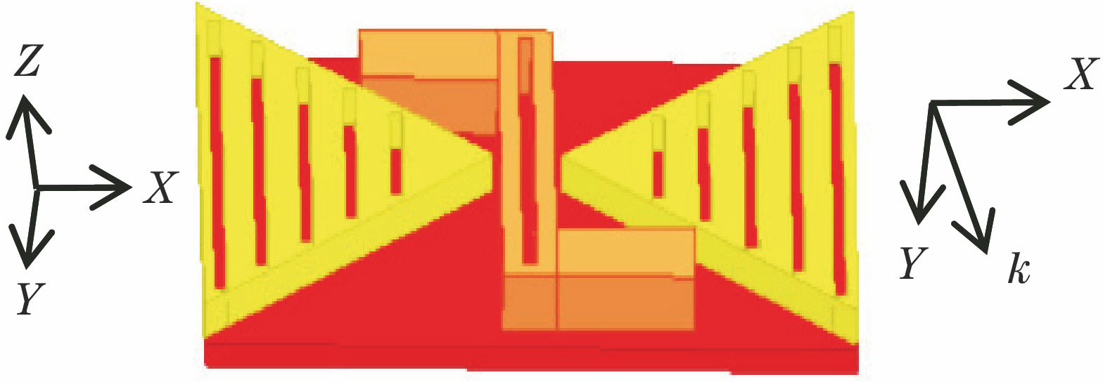
    Fig. 1. Multi-slot butterfly dipole
    Schematics of unit structure. (a) Y-Z view; (b) X-Y view
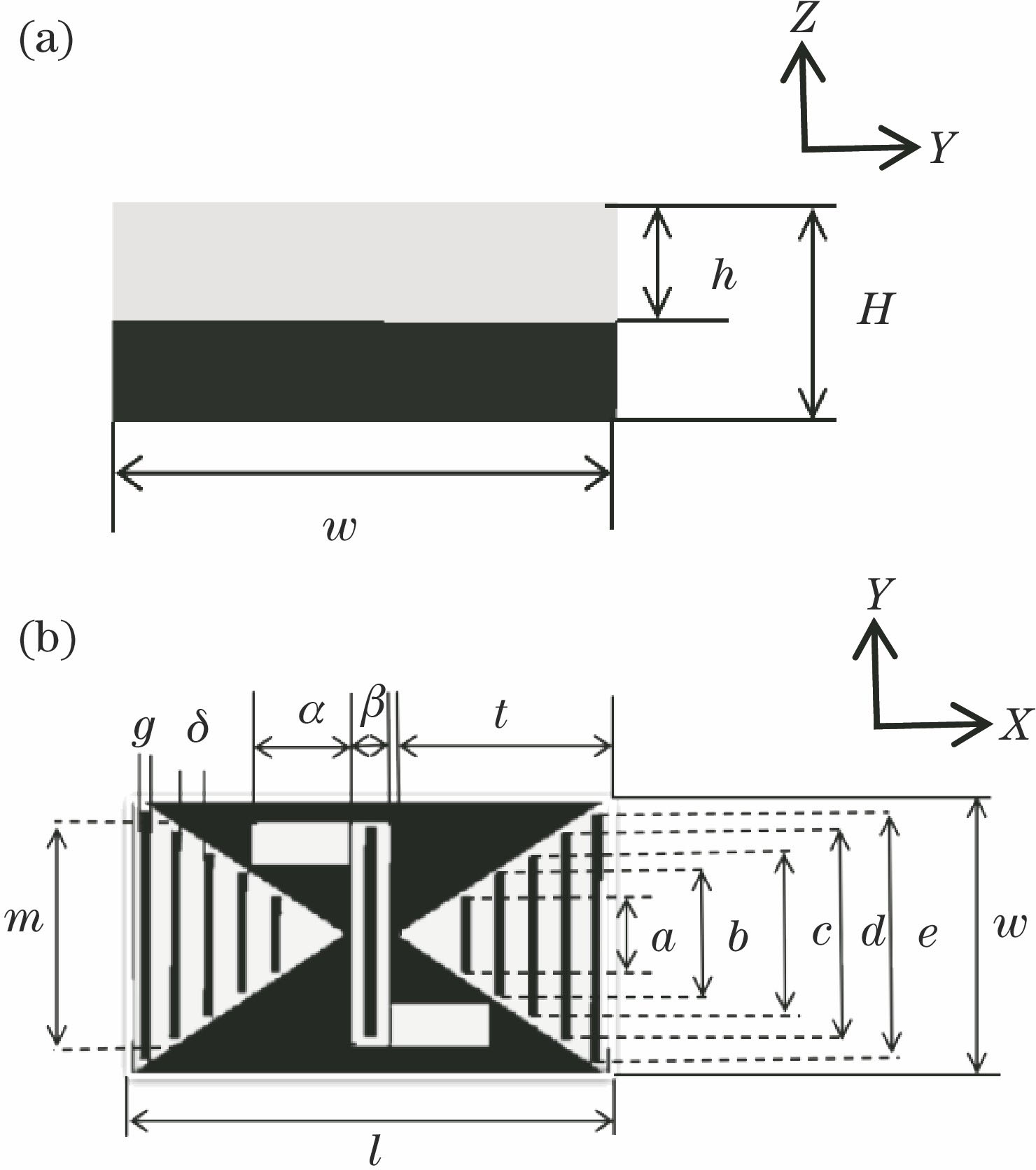
    Fig. 2. Schematics of unit structure. (a) Y-Z view; (b) X-Y view
    Electric field Ex distributions in plane at z=0 nm. (a) λ=880 nm, multi-slot butterfly dipole; (b) λ=1200 nm, multi-slot butterfly dipole; (c) λ=880 nm, butterfly dipole; (d) λ=1200 nm, butterfly dipole; (e) absorption characteristics of multi-slot butterfly dipole and butterfly dipole
    Fig. 3. Electric field Ex distributions in plane at z=0 nm. (a) λ=880 nm, multi-slot butterfly dipole; (b) λ=1200 nm, multi-slot butterfly dipole; (c) λ=880 nm, butterfly dipole; (d) λ=1200 nm, butterfly dipole; (e) absorption characteristics of multi-slot butterfly dipole and butterfly dipole
    Electric field Ex distributions in plane at z=0 nm for λ=1000 nm. (a) Seamless; (b) slot number n=2; (c) slot number n=4; (d) slot number n=6; (e) slot number n=8; (f) slot number n=10
    Fig. 4. Electric field Ex distributions in plane at z=0 nm for λ=1000 nm. (a) Seamless; (b) slot number n=2; (c) slot number n=4; (d) slot number n=6; (e) slot number n=8; (f) slot number n=10
    Electric field Ex distributions in plane at z=0 nm for λ=1450 nm. (a) Without nanowires; (b) with nanowires; (c) absorption characteristics of two classes of structures
    Fig. 5. Electric field Ex distributions in plane at z=0 nm for λ=1450 nm. (a) Without nanowires; (b) with nanowires; (c) absorption characteristics of two classes of structures
    Absorption characteristics of different materials. (a) Absorptivity; (b) average absorptivity
    Fig. 6. Absorption characteristics of different materials. (a) Absorptivity; (b) average absorptivity
    Multi-slot butterfly dipole nano-antenna
    Fig. 7. Multi-slot butterfly dipole nano-antenna
    (a) Absorption spectrum and (b) reflectance spectrum of multi-slot butterfly dipole nano-antenna; electric field Ex distributions of multi-slot butterfly dipole nano-antenna array in plane at z=0 nm plane for (c) λ=680 nm, (d) 880 nm, (e) 1080 nm, (f) 1200 nm, (g) 1450 nm and (h) 1680 nm
    Fig. 8. (a) Absorption spectrum and (b) reflectance spectrum of multi-slot butterfly dipole nano-antenna; electric field Ex distributions of multi-slot butterfly dipole nano-antenna array in plane at z=0 nm plane for (c) λ=680 nm, (d) 880 nm, (e) 1080 nm, (f) 1200 nm, (g) 1450 nm and (h) 1680 nm
    Schematic of nano-antenna central gap distance and absorption characteristics under different distances. (a) Schematic; (b) absorptivity; (c) average absorptivity
    Fig. 9. Schematic of nano-antenna central gap distance and absorption characteristics under different distances. (a) Schematic; (b) absorptivity; (c) average absorptivity
    Electric field Ex distributions in plane at z=0 nm for λ=800 nm. (a) D=80 nm; (b) D=100 nm; (c) D=120 nm; (d) D=140 nm
    Fig. 10. Electric field Ex distributions in plane at z=0 nm for λ=800 nm. (a) D=80 nm; (b) D=100 nm; (c) D=120 nm; (d) D=140 nm
    Absorption characteristics under different slot numbers n. (a) Absorptivity; (b) average absorptivity
    Fig. 11. Absorption characteristics under different slot numbers n. (a) Absorptivity; (b) average absorptivity
    Absorption characteristics under different film thicknesses h. (a) Absorptivity; (b) average absorptivity
    Fig. 12. Absorption characteristics under different film thicknesses h. (a) Absorptivity; (b) average absorptivity
    Influences of (a) polarization angle and (b) inclined incidence angle on absorption characteristics
    Fig. 13. Influences of (a) polarization angle and (b) inclined incidence angle on absorption characteristics
    ParameterValue /nm
    l1020
    w800
    m750
    g30
    h450
    α240
    β120
    t440
    δ240
    H750
    a200
    b300
    c400
    d550
    e650
    Table 1. Parameter setting
    Nano-antenna structureAbsorption band /nmAverage absorptivity /%
    Spiral nano-antenna[12]400-160074.9
    Slot Yagi nano-antenna[10]400-150060
    U shaped nano-antenna[11]400-140052
    Dipole nano-antenna[9]400-85030
    Table 2. Absorptivity of single structure nano-antenna
    Yuanyuan Liu, Kangkang Li, Xiaomeng Tian, Lu Zhu. Design and Absorption Characteristics of Multi-Slot Butterfly Dipole Nano-Antenna[J]. Acta Optica Sinica, 2019, 39(2): 0223002
    Download Citation