【AIGC One Sentence Reading】:Driven by data transmission demands, we've developed a versatile optical switch using asymmetric Y-junctions and MMI couplers on a polymer waveguide. It offers mode-insensitive and mode-selective switching, low power consumption, and scalability for MDM systems.
【AIGC Short Abstract】:Driven by the growing data transmission needs, we developed a versatile optical switch using asymmetric Y-junctions and MMI couplers on a polymer waveguide. It offers both mode-insensitive and mode-selective switching, exhibiting low insertion loss and high extinction ratio with minimal power consumption. This innovative device promises scalable and flexible support for multiple spatial modes, vital for advancing MDM systems.
Note: This section is automatically generated by AI . The website and platform operators shall not be liable for any commercial or legal consequences arising from your use of AI generated content on this website. Please be aware of this.
Abstract
Driven by the large volume demands of data in transmission systems, the number of spatial modes supported by mode-division multiplexing (MDM) systems is being increased to take full advantage of the parallelism of the signals in different spatial modes. As a key element for photonic integrated circuits, the multimode waveguide optical switch (MWOS) is playing an important role for data exchange and signal switching. However, the function of the traditional MWOS is simple, which could only implement the mode-insensitive or mode-selective switching function; it is also difficult to scale to accommodate more spatial modes because of the limitation of the device structure. Therefore, it is still challenging to realize a multifunctional and scalable MWOS that could support multiple modes with low power consumption and high flexibility. Here, we propose and experimentally demonstrate a multifunctional MWOS based on asymmetric Y-junctions and multimode interference (MMI) couplers fabricated on a polymer waveguide platform. Both mode-insensitive and mode-selective switching functions can be achieved via selectively heating different electrode heaters. The fabricated device with the total length of shows an insertion loss of less than 12.1 dB, and an extinction ratio of larger than 8.4 dB with a power consumption of for both mode-insensitive and mode-selective switching functions, at 1550 nm wavelength. The proposed MWOS can also be scaled to accommodate more spatial modes flexibly and easily, which can serve as an important building block for MDM systems.
1. INTRODUCTION
To meet the ever-increasing demands of data transmission capacity, optical communication has been developed rapidly [1–5]. Various multi-dimensional multiplexing technologies have been investigated and applied in optical communication systems, such as polarization-division multiplexing [6–8], time-division multiplexing [9–11], wavelength-division multiplexing [12–14], and mode-division multiplexing (MDM) [15–18]. Among them, MDM technology is an emerging technology to accommodate the increasing demands for the capacity of optical communication systems, which can enhance the link capacity by multiplexing multiple spatial modes orthogonal to each other [19–21]. In addition, only a single wavelength carrier is needed in an MDM system, which not only simplifies the complexity of the system but also reduces the power consumption and the cost.
Several key building blocks have been presented for realizing MDM systems, such as mode (de)multiplexers [22], high-order mode filters [23], multimode waveguide bends [24], multimode 3-dB splitters [25], and multimode optical switches [26]. Among them, multimode optical switches control the switching states of different mode channels, which are indispensable in an MDM system. Compared to an optical switch used for a single-mode waveguide system, a multimode optical switch suffers from modal crosstalk among different spatial modes, a greater vulnerability to radiation loss, and mode distortion. Therefore, the realization of a multimode optical switch is still very challenging. Recently, there have been growing research efforts to develop a high-performance multimode optical switch to embrace MDM applications. Among the various types of multimode optical switches, the multimode waveguide optical switch (MWOS) has received extensive attention because it can be easily integrated with other waveguide-based devices and be also mass produced; in addition, it offers much flexibility in structure design and material choice [27,28].
Polymer waveguide platform is deemed as a promising platform for photonic integrated circuits (PICs) for the realization of optical interconnect and optical communication because of their particular advantages of compatibility with CMOS and fiber [29–32]. Moreover, it is enormously attractive for fabrication convenience and low cost [33–36]. Currently, polymer materials have been widely utilized for realizing MWOS due to their high thermo-optic (TO) coefficient and low thermal conductivity. Several polymer MWOSs have been demonstrated to realize MDM systems [37–40]. The mode-selective switch using directional couplers, which supports three spatial modes, has been proposed and experimentally demonstrated [41]. In our previous work, we have also developed a mode-insensitive polymer TO switch that has extinction ratios of larger than 13.1 dB with a driving power of 5.9 mW for the and modes, over the wavelength range of the band [42]. Several mode-insensitive optical switches for four spatial modes have also been reported in recent years [43,44]. The mode-insensitive switching can effectively reduce the power consumption, but has less flexibility than the mode-selective switching. Therefore, it is necessary to design an MWOS to realize both mode-insensitive and mode-selective switching functions, which not only will provide more flexible switching functions but also decrease the power consumption. Moreover, to fully exploit the capacity of MDM systems, there is a strong need to develop a high-performance MWOS, which can be easily scaled to accommodate more high-order modes.
Sign up for Photonics Research TOC. Get the latest issue of Photonics Research delivered right to you!Sign up now
In this paper, we propose and experimentally demonstrate a multifunctional MWOS on the polymer waveguide platform, which could achieve both mode-insensitive and mode-selective switching functions for , , , and modes by combining two asymmetric Y-junctions with two multimode interference (MMI) couplers. The asymmetric Y-junction at the input end is used to convert the input mode into or mode and transmit it into one of the two branches, and the MMI coupler is used to enable mode-insensitive switching for and modes. Besides, three electrode heaters are adopted to achieve the three switching functions. For mode-insensitive switching, all the four modes launched into the MWOS can be switched between “On” and “Off” states simultaneously at the output end by driving the electrode heater in the middle of the two MMI couplers. For mode-insensitive switching, the measured insertion losses of the four modes are all less than 13.5 dB in the wavelength range of 1500–1600 nm. The measured extinction ratios are larger than 8.4 dB for all the four guided modes with the power consumption of in the wavelength range of 1500–1600 nm, and the switching times are for each mode. Moreover, the fabricated device can also implement the mode-selective switching functions well. The proposed MWOS not only decreases the power consumption effectively, but also implements a flexible switching function, which can be widely used in MDM systems.
2. DEVICE DESIGN AND WORKING PRINCIPLE
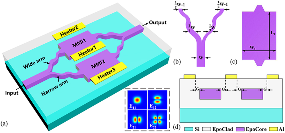
The proposed multifunctional MWOS is designed on the polymer waveguide platform by using EpoClad () as the cladding material and EpoCore () as the core material, respectively. As shown in Fig. 1(a), the proposed MWOS consists of two asymmetric Y-junctions, four tapered waveguides, four S-bends, and two MMI couplers, where the tapered waveguides and S-bends are used to connect asymmetric Y-junctions and MMI couplers. The asymmetric Y-junction at the input end is used as a mode splitter and the one at the output end is used as a mode combiner. Moreover, the two MMI couplers have the same structural size and are used as the mode-insensitive switches for and modes.
Figure 1.(a) Schematic diagram of the proposed device. Enlarged view for (b) the asymmetric Y-junction and (c) the MMI coupler. (d) Cross-section for the modulation region.
Figure 1(b) shows the schematic structure of the asymmetric Y-junction, and the width of the input waveguide () is designed to be 10 μm. The widths of the wide arm and the narrow arm of the asymmetric Y-junction are and , respectively, with S-bends extending over a distance 1600 μm to a separation of 10 μm. Besides, a tapered waveguide with a length of 120 μm and a S-bend with a width of and a length of 1000 μm are adopted to connect asymmetric Y-junction and MMI coupler. The MMI coupler connected to the wide arm of asymmetric Y-junction is MMI-1, and the one connected to the narrow arm is MMI-2. Figure 1(c) shows the schematic diagram of the MMI coupler, where two tapered waveguides with a gradual increase width from 5 μm to 10 μm and a length of 450 μm are inserted at the input and output ends of the multimode waveguide to enhance the output efficiency and reduce the scattering loss [45]. The operation of an MMI device is based on the self-imaging effect in a multimode waveguide, where the guided mode is excited in the multimode waveguide and reproduced at certain specific longitudinal locations periodically along the direction of waveguide propagation as single or multiple images [46,47]. To support sufficient modes, the width of the multimode waveguide () is determined to be 25 μm. The length of the multimode waveguide () is optimized to be 790 μm, corresponding to the distance needed to form the first one-folded image. The cross-section diagram of the modulation section of the MWOS is shown in Fig. 1(d). The thicknesses of the core layer, upper cladding, and lower cladding are 9 μm, 6 μm, and 6 μm, respectively. The simulated mode profiles of the input waveguide for an operation wavelength of 1550 nm are shown in the insets of Fig. 1(a), where the mode fields are well confined in the core of the waveguide. To achieve the mode-insensitive switching function by heating only one electrode, we place the electrode heaters on the side of the two MMIs, as shown in Fig. 1(a), which is also helpful to reduce the thermal crosstalk when the mode-selective switching function is performed. The electrode heater in the middle of the two MMI couplers is Heater-1, the one near MMI-1 is Heater-2, and the one near MMI-2 is Heater-3. The width of all the three electrode heaters is 10 μm and the length of them is also . To achieve both large extinction ratio and low power consumption, the electrode heaters are placed at 2 μm away from the MMI couplers (μ). The distance between Heater-1 and Heater-2, as well as Heater-1 and Heater-3, is 29 μm.
The operation principle of the MWOS is described as follows. First, the mode-insensitive switching function is investigated and presented with Heater-2 and Heater-3 turned off. Heater-1 is adopted to implement the mode-insensitive switching function, which is located between MMI-1 and MMI-2 and can modulate both MMI switches at the same time. Referring to the schematic diagram in Fig. 1(a), the asymmetric Y-junctions are used as the mode splitter and combiner, which provides a large bandwidth [48,49]. For the () mode launched into the input port of the device, it will evolve adiabatically into the () mode in the wide arm of the asymmetric Y-junction and transmit into MMI-1. For the () mode launched into the input port of the device, it will evolve adiabatically into the () mode in the narrow arm of the asymmetric Y-junction and transmit into the MMI-2. When Heater-1 is turned off, because the MMI coupler is designed to form the first one-folded image at the output end, the light is output from the MMI coupler and transported into the asymmetric Y-junction at the output end to evolve into the original mode, where the device is in the “On” state. To achieve the “Off” state of the switch, the interference effect and self-image effect in the multimode waveguide can be broken and changed through the TO effect, and the output end of the multimode waveguide will no longer form the first one-folded image. To estimate the driving temperature and switching power of the design, we apply the built-in electrode heater model in the 3D finite-difference beam propagation method (RSoft 3DFD-BPM, Synopsys, Sunnyvale, CA) and calculate the optical transmission of the switch as a function of the driving temperature, where the TO coefficient of the polymer material is taken to be [50]. Figure 2(a) shows the thermal field distribution of the device when Heater-1 is turned on. It can be observed that both of the MMI couplers can be heated by Heater-1. Figure 2(b) shows the simulated optical transmission of the MWOS as a function of the driving temperature of Heater-1 (), and it can be observed that the transmission trends of all four modes with are almost the same. It is also clear that the driving temperature to achieve the “OFF” state of the device is for all the four modes, and the extinction ratios for each mode at the 1550 nm wavelength are 30.0 dB, 27.5 dB, 23.9 dB, and 20.2 dB, respectively. Moreover, the insertion losses for each mode are 0.06 dB, 0.09 dB, 0.05 dB, and 0.18 dB, respectively. The propagation paths and the optical field distribution for each case of the device are shown in Fig. 2(d). The simulated transmission spectra of the device are shown in Fig. 2(c), which indicates that our design is wavelength independent. It is observed from the simulation results that the extinction ratios are larger than 16.8 dB and the insertion losses are less than 0.26 dB for each mode in the wavelength range of 1500 nm to 1600 nm. By turning on or off Heater-1, our device can realize the mode-insensitive switching function well.
Figure 2.(a) Thermal field distribution of the device when Heater-1 is turned on. (b) Simulated transmission of the , , , and modes as a function of . (c) Simulated transmission spectra of the , , , and modes as a function of the wavelength. (d) Simulated propagation results at 1550 nm wavelength for each mode individually.
Next, the mode-selective switching functions of the device are investigated. Heater-2 is adopted to implement the first mode-selective switching function with Heater-1 and Heater-3 turned off. Figure 3(a) shows the thermal field distribution of the device when Heater-2 is turned on, and it can be observed that only MMI-1 can be heated and modulated. Therefore, the effective index of MMI-1 changes due to the TO effect and the modes in MMI-1 ( and modes) will be modulated. Since the distance between Heater-2 and MMI-2 is far, the effective index of MMI-2 does not change, and the modes in MMI-2 ( and modes) will not be modulated. Figure 3(b) shows the simulated optical transmission of the MWOS as a function of the driving temperature of Heater-2 (). It can be observed that the output optical powers of the mode and mode decrease and then increase with an increase of ; however, the output optical powers of mode and mode keep almost unchanged. It can be concluded from the simulation results that the extinction ratios for the and modes at the 1550 nm wavelength are 31.2 dB and 27.7 dB with , respectively. Next, the second mode-selective switching function is investigated with Heater-1 and Heater-2 turned off. Figure 3(c) shows the thermal field distribution of the device when Heater-3 is turned on, and it can be observed that only MMI-2 can be heated and modulated. Figure 3(d) shows the simulated optical transmission of the MWOS as a function of the driving temperature of Heater-3 (), and the simulation results show the extinction ratios for the and modes at the 1550 nm wavelength are 25.0 dB and 43.9 dB with , respectively. As a result, our design can implement the mode-insensitive and mode-selective switching functions well by selectively turning on or off the electrode heaters.
Figure 3.(a) Thermal field distribution of the device when Heater-2 is on. (b) Simulated transmission of the , , , and modes as a function of . (c) Thermal field distribution of the device when Heater-3 is on. (b) Simulated transmission of the , , , and modes as a function of .
We fabricated the MWOS following the designed parameters by using the in-house microfabrication facilities, as shown in Fig. 4(a). First, a 6 μm thick EpoClad was spin-coated onto the Si substrate to build the lower cladding. Then the chip was prebaked at 120°C for 5 min to remove excess solvents; after that, it was exposed to ultraviolet (UV) light generated by a UV lithography machine (ABM-USA Inc., San Jose, CA) at for 10 s and hard-baked at 120°C for 30 min to enhance the material cross-linking. Next, a 9 μm thick EpoCore negative photopolymer was spin-coated onto the lower cladding and prebaked at 50°C for 2 min and 90°C for 4 min, and then the patterns of MWOS waveguides were transferred to the EpoCore film by UV photolithography for 8 s. Subsequently, the sample was post-baked at 50°C for 2 min and 85°C for 4 min, and then ramped down to room temperature. The unexposed EpoCore was removed with a developer solution for 60 s and washing with isopropyl alcohol and deionized water; after that, the sample was hard-baked at 120°C for 30 min to enhance the adhesion between core layer and the lower cladding layer. The microstructures of the asymmetric Y-junction and MMI couplers are shown in Fig. 4(b) and Fig. 4(c), respectively. It can be observed that the boundaries of the waveguides are clear and can guarantee the mode evolution and transmission. Next, a 10 μm thick EpoClad film was spin-coated and cured, covering the waveguide core as upper cladding. Finally, a 200 nm thick Al film was deposited onto the chip by thermal evaporation, and the electrode heaters were then patterned by UV photolithography and wet etching. The top-view morphology of the device is shown in Fig. 4(d), and it can be observed that the electrode heaters are precisely loaded on the same position as the design. Figure 4(e) shows the cross-section microscope image of the fabricated MWOS, where the waveguide dimensions are suitable with the designed values. The total length of the fabricated MWOS is .
Figure 4.(a) Steps in the fabrication of the proposed MWOS with polymer materials. The top-view microscope images of (b) the asymmetric Y-junction and (c) the MMI couplers. Microscope images of (d) the electrode heater and (e) an end face of the fabricated device.
We characterized the performance of the fabricated MWOS by using the established few-mode optical waveguide testing system. For our fabricated device, we launched the , , , or mode into the input waveguide with a lensed fiber and a tunable semiconductor laser (TSL-510, Santec, Komaki, Japan). We excited the mode by launching the light exactly at the center of the input waveguide. The , and modes can be preferentially excited to a high purity by properly adjusting the position and the tilt angle of the laser beam incident into the input waveguide with the help of a five-degree micro-positioner. The output power of the device was detected with an optical power meter (2832-C, Newport Corp., Irvine, CA) through a few-mode fiber, and the output mode patterns of the device were captured by an infrared charge-coupled device (CCD) camera (C2741-03, Hamamatsu, Hamamatsu-city, Japan). To modulate the device, two metal probes are used to apply the driving voltage to the electrode heaters.
First, the mode-insensitive switching function is investigated. Figure 5(a) shows the measured output power versus driving power of Heater-1 () of the fabricated device. The initial state of the MWOS is the “On” state (), for the , , and modes, and our device exhibits insertion losses of 11.4 dB, 11.7 dB, 11.6 dB, and 12.1 dB at a 1550 nm wavelength, respectively. The “Off” state of the device arrives with a power consumption of , and the measured extinction ratios are 10.6 dB, 9.1 dB, 9.0 dB, and 10.0 dB, respectively, at 1550 nm wavelength. Figure 5(b) shows the measured transmission spectra when the device is working at its “On” and “Off” states for the four modes. With the wavelength range of 1500–1600 nm, the measured insertion losses are less than 12.9 dB, 13.5 dB, 11.7 dB, and 12.7 dB for each mode, and the measured extinction ratios are larger than 8.5 dB, 8.4 dB, 8.4 dB, and 9.8 dB for each mode, respectively. We can improve the performance by optimizing the fabrication process of the device and introducing polymer materials with a low absorption loss [51]. Moreover, we can further reduce the insertion loss of the device by polishing the end face of the waveguide and packaging the device [52]. The near-field images with different collected by CCD camera are shown in Fig. 5(c). It can be clearly observed that the output power decreases with increasing from 0 mW to 32.5 mW. It can be concluded that our device is wavelength independent and can work in a large bandwidth.
Figure 5.(a) Measured transmission of the , , , and modes as a function of . (b) Measured transmission spectra of the , , , and modes as a function of the wavelength. (c) Output near-field photos with different when , , , or mode was launched into the device at the 1550 nm wavelength.
Next, the mode-selective switching functions are characterized. The measured output power of the fabricated MWOS as a function of the driving power applied on Heater-2 () is shown in Fig. 6(a). Compared to the simulation results shown in Fig. 3(b), the measured results show that the and modes also change slightly with , which is mainly due to a slight deviation in the experimental preparation of the asymmetric Y-junction. When the or mode is launched into the device, it is not fully evolved into the narrow branch of the asymmetric Y-junction, but there is a small part of the light coupled into the wide branch that will be modulated. Therefore, the output power will also be changed as the or mode is launched into the device. This problem can be solved by optimizing the fabrication process. For the first mode-selective switching function, the measured extinction ratios for the and modes at 1550 nm wavelength are 8.4 dB and 8.8 dB with a power consumption of 32.1 mW, respectively. The output near-field images of the device with different are shown in Fig. 6(b), which is consistent with the simulation results. For the second mode-selective switching function, the measured results are shown in Figs. 6(c) and 6(d). As previously stated, the and modes keep almost unchanged with the driving power applied on Heater-3 (), and the extinction ratios for the and modes at 1550 nm wavelength are 8.5 dB and 8.4 dB with a power consumption of 32.6 mW, respectively. The output near-field images with different are shown in Fig. 6(d).
Figure 6.(a) Measured transmission of the , , , and modes as a function of . (b) Output near-field photos with different when the , , , or modes were launched into the device at the 1550 nm wavelength. (c) Measured transmission of the , , and modes as a function of . (d) Output near-field photos with different when , , , or mode was launched into the device at the 1550 nm wavelength.
We also measured the response time of the MWOS by modulating the electrode heater with a 100 Hz square-wave controlling signal generated from a function generator (SDG6052X, SIGLENT, Shenzhen, China) and detecting the output signals with a photodetector and a digital oscilloscope (DS4024, RIGOL, Suzhou, China). The measured response time for each mode is shown in Fig. 7, where the upper waveform is the original square-wave controlling signal and the lower waveform is the response of optical signal from the device. For the mode launched into the device, the detected response exhibits a rise time and fall time of 1.44 ms and 1.48 ms, and those for mode, mode, and mode are 1.76 ms and 1.64 ms, 1.68 ms and 1.72 ms, and 1.48 ms and 1.52 ms, respectively. The response time of the switch can be improved by employing the polymer/silica hybrid waveguide structure, which uses silica as the lower cladding for quicker removal of the heat from the core by the Si substrate [53]. Despite a relatively low speed of our polymer waveguide device, it can be used in cost-effective scenarios where the switching speed is not required. The polymer platform is an attractive option for implementing switches due to the advantages of low power consumption, low cost, and simple fabrication.
Figure 7.Measured dynamic switching of the proposed MWOS when the (a) , (b) , (c) , and (d) modes were launched into the device.
The proposed switch scheme can be scaled for more higher-order modes. Figure 8 shows a schematic structure of an eight-mode multifunctional multimode switch, which consists of two asymmetric Y-junctions and four MMI couplers with the same structural size. The input and output waveguides of the switch are designed to support the , , , , , , , and modes. For the () mode launched into the switch, it will transmit into Branch-2 of the asymmetric Y-junction with the mode remaining unchanged, and then transmit into MMI-2. For the () mode launched into the switch, it will evolve adiabatically into the () mode in Branch-3, and then transmit into MMI-3. For the () mode launched into the switch, it will evolve adiabatically into the () mode in Branch-1, and then transmit into MMI-1. And for the () mode launched into the switch, it will evolve adiabatically into the () mode in Branch-4, and then transmit into MMI-4. After that, the MMI couplers are used to enable the mode-insensitive switching function for the and modes. Heater-5 is used to implement the mode-insensitive switching function for all eight modes, and Heater-1, Heater-2, Heater-3 and Heater-4 are used to implement the mode-selective switching functions.
Figure 8.Schematic structure of an eight-mode multifunctional switch.
In conclusion, a multifunctional polymer TO MWOS with low power consumption and a large bandwidth is essential for an MDM system. Conventional switches have a single function and narrow bandwidth due to the structural limitations. In this work, a multifunctional MWOS with a 100 nm bandwidth is theoretically designed and experimentally demonstrated, which can implement both mode-insensitive and mode-selective switching functions for the , , , and modes. For the mode-insensitive switching function, the measurement results exhibit insertion losses of less than 13.5 dB and extinction ratios of larger than 8.4 dB for all the four modes, within the 1500–1600 nm wavelength range. The switching rise time and fall time of the polymer MWOS are for each mode. Besides, the mode-selective switching functions are also well implemented. The power consumption of the device is to achieve both mode-insensitive and mode-selective switching functions. By using two asymmetric Y-junctions integrated with N MMI couplers (, 4, and 5), the proposed switching scheme can be scaled for more higher-order modes. Such a high-performance MWOS is advantageous to realize multimode PICs in the future and can effectively improve the system transmission capacity.
 AI Video Guide
  AI Picture Guide
 AI One Sentence