
Zhishan GAO, Qun YUAN, Yifeng SUN, Jianqiu MA, Zhenyan GUO, Dan ZHU, Yuqing ZHAO, Xiao HUO, Shumin WANG, Jiale ZHANG, Xing ZHOU, Chunxia WU, Xiaoxin FAN. Non-destructive Test Methods of Microstructures by Optical Microscopy(Invited)[J]. Acta Photonica Sinica, 2022, 51(8): 0851501
- Acta Photonica Sinica
- Vol. 51, Issue 8, 0851501 (2022)
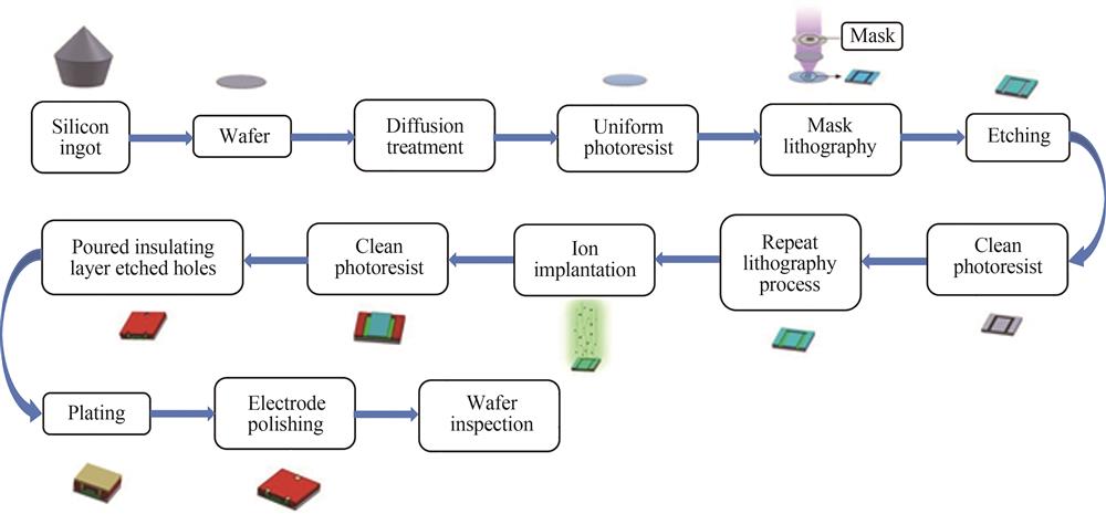
Fig. 1. Single-layer manufacturing process flow chart in the main manufacturing process of semiconductor chips
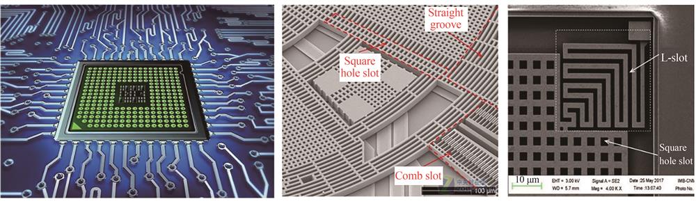
Fig. 2. Common chip structure diagram
Fig. 3. Diagram of surface texture on high pressure seals
Fig. 4. Diagram of micro-structure on super-lens element
Fig. 5. Harmful micro-structure diagram
Fig. 6. Schematic of dark field off-axis illumination light path
Fig. 7. Schematic of confocal microscopy imaging optical path
Fig. 8. Schematic diagram of spectral inversion and through-focus scanning
Fig. 9. Optical path schematic of low-coherence interferometric microscope
Fig. 10. “Snake” motion scanning route
Fig. 11. Physical map of the internal microscopic parts of the dark-field inspection equipment
Fig. 12. Defect detection results of Nd glass with dark field microscopy machine vision
Fig. 13. Texture defect results in TFT displays
Fig. 14. Three-dimensional topography detection results by confocal microscopy
Fig. 15. 3D topography of super-lens by white light low-coherence interferometric microscope
Fig. 16. The detection result curve of the bat wing effect
Fig. 17. White light interference fringe envelope and detect results with or without batwing-effect influence
Fig. 18. The diagram of W/3 metrology rule in ISO5436-1:2000(E)and simulation results of coupling distance of groove samples
Fig. 19. Two different modes of Linnik interference microscope
Fig. 20. Results of CD and its error between the TSOM combined with machine-learning and SEM for six samples
Fig. 21. Comparison of comb tooth groove structure tomography of a silicon MEMS sensor between SEM and self-developed instrument
Fig. 22. Comparison of equal-cycle grating structure tomography between SEM and self-developed instrument
Fig. 23. The photo of reflective nondestructive measuring system instrument with near-infrared Linnik-type interferometric microscope
Fig. 24. Images of single-groove on silicon-base with 200 μm depth imaged by Linnik-type interferometric microscope
| |||||||||||
Table 1. Measurement results of spectral-inversion and through-focus scanning method

Set citation alerts for the article
Please enter your email address
© Copyright 2018-2021 | Chinese Laser Press. All Rights Reserved 沪ICP备15018463号-20