
Jingzhong Yang, Michael Zopf, Fei Ding. Strain tunable quantum dot based non-classical photon sources[J]. Journal of Semiconductors, 2020, 41(1): 011901
- Journal of Semiconductors
- Vol. 41, Issue 1, 011901 (2020)
Abstract
1. Introduction
The on-demand generation of single photons and entangled photon pairs are of fundamental interest for many applications such as quantum repeaters[
Semiconductor quantum dots (QDs) are the most promising candidate to generate single photons and entangled photon pairs truly on-demand. These so-called ‘artificial atoms’ exhibit discrete electronic states with excitonic transitions, providing means for high efficiency, deterministic emission[
However, ‘no two snowflakes are alike’ is a principle that also seems to hold for QDs. Their growth is governed by randomness in shape, material composition, and internal strain fields. This inability to grow perfect QDs is a major challenge: As an example, key elements in quantum information processing[
In this review, we recapitulate the development and achievements for the strain tuning of III–V QDs. We start by introducing the effect of external biaxial stress on a QDs containing nanomembrane placed on a piezoelectric actuator[
2. Strain-engineering of semiconductor quantum dots
To understand the energy band structure and optical properties of semiconductors, k·p perturbation theory is commonly employed[
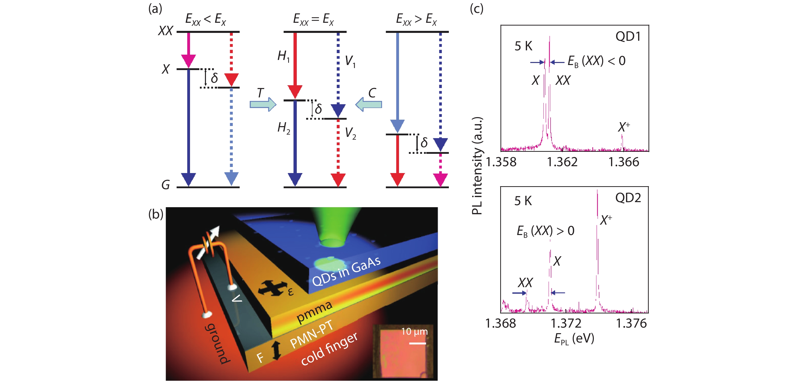
Fig. 1 shows the effect of strain on InGaAs/GaAs QDs attached to a biaxial piezoelectric actuator that induces. The QD sample is grown by MBE along the [001] crystal direction on a GaAs substrate. The self-assembled InGaAs QDs are embedding in layers of GaAs, grown on top of AlGaAs sacrificial layer. Square patterns are defined in the sample by photolithography. Making use of the selective etching of the sacrificial layer with diluted hydrofluoric acid, the nanomembranes are released and become free-standing on the substrate. They are then transferred on a 300 μm thick piezoelectric [Pb(Mg1/3Nb2/3)O3]0.72-[PbTiO3]0.28 (PMN-PT), allowing for the application of large, biaxial in-plane strain fields at low temperature. As illustrated in Fig. 1(b), PMMA is used as an adhesive layer between the QD membranes and the piezoceramic[
![]()
Figure 1.(Color online) (a) Scheme of the cascade emission of the
In Figs. 2(a) and 2(c), the PL spectra of QD1 and QD2 are shown as a function of the voltage applied to the PMN-PT actuator. The voltage is swept between 0 to 1100 V with steps of 20 V. When the voltage is positive, an in-plane compressive strain is always applied on the QDs membrane, resulting in a blueshift of up to ~1.8 meV. Then, the effect of biaxial strain on the binding energy binding energies EB(XX) and EB(X+) relative to X is investigated for the different dots. As shown in Figs. 2(b) and 2(d), both the EB(XX) and EB(X+) monotonically increase with a constant slope while the X emission is blue shifted. By means of empirical pseudopotential calculations, this effect is attributed to an increase in electron-hole Coulomb interaction upon compressive biaxial stress. Furthermore, the FSS keeps constant while tuning the voltage, as confirmed by the calculations[
![]()
Figure 2.(Color online) PL spectra of (a) QD1 and (c) QD2 as a function of applied voltage on the PMN-PT actuator. The linear increase of
Therefore, biaxial strain tuning is a reliable method to engineer the QD electric structure in a precise and reversible way. Excitonic emission wavelengths are controlled and color coincidence between X and XX photons can be achieved. The possibility to tune the photon emission wavelength can resolve the scalability difficulty via the specific strain applied to the different QD sources. On the other hand, the demonstration of strain tuning also contributes to the investigation of other material systems such as 2D graphene[
3. Wavelength tuning of single photons from a light emitting diode
Semiconductor QDs have the inherent advantages of integrability with the mature semiconductor technologies that have matured in the research and industry. Electrically driven single-photon sources (SPs) based on QDs helps to simplify the bulky laser excitation system and make QDs more valuable for the use in on-chip quantum devices[
Fig. 3(a) shows the sketch of a wavelength-tunable, electrically triggered light-emitting diode (LED) device containing InGaAs/GaAs QDs grown by MBE. The QDs are embedded between a n- and p- doped GaAs layers. Nanomembranes are fabricated and transferred on the PMN-PT via gold-gold thermo-compression bonding, allowing for the application of in-plane biaxial strain on the QDs. The electric triggering is implemented by applying a DC bias Vd and a 300 ps consecutive electrical pulse Vpp (see Fig. 3(c)). Another DC bias Vp is applied to the piezoelectric actuator, sharing a common ground connection with the triggering part. A microscope objective is located on top of the sample and collects the emitted photon emission. A sketch of the complete device is illustrated in Fig. 3(a). The microscope image in Fig. 3(b) shows the electrical bonding on top of the n-GaAs nanomembrane via aluminum wires[
![]()
Figure 3.(Color online) Sketch and characterization of a nanomembrane-based strain tunable single- photon-emitting diode. (a) n–i–p diode nanomembrane containing InGaAs/GaAs QDs bonded on a PMN-PT crystal via gold-to-gold thermo-compression bonding. The p-contact of the nanomembrane and the PMN-PT share a common ground. A diode voltage
A sequence of optical characterization measurements is implemented to demonstrate that this LED allows for adjusting the wavelength of photon emission which is effectively triggered by ultrashort electric pulses. Fig. 3(d) shows a group of electroluminescence (EL) spectra for different DC voltage amplitude. The emission peaks are distinguished with polarization-resolved EL measurements. It is also apparent that the decay time of X photon emission gets altered with the changing of Vd (Fig. 3(e)). This is ascribed to the reduced time jitter at a low DC bias because of the band bending[
Apart from the investigation of electrically triggered QDs, their strain tunability in the nanomembrane is also studied, while keeping the single-photon emission properties. In Fig. 4(a), the EL-spectrum series as a function of different electric field Fp is implemented by controlling the voltage Vp. The X photon emission line shows a blueshift with the Fp changed from –10 to 20 kV/cm. To demonstrate single-photon emission, the second-order autocorrelation function g(2)(τ) is measured for the X emission and shown in Figs. 4(b)–4(d). As evident from the results, the single-photon purity is maintained under different strain conditions at the QD. Therefore, electrically triggered QDs can provide a stable single-photon emission with a precisely adjustable wavelength.
![]()
Figure 4.(Color online) (a) Tunable
4. Strain tuning of light-hole excitons
Semiconductor QDs predominantly allow for the formation of excitonic complexes based on heavy-holes. In contrast, light-hole excitons are quasiparticles formed by a single electron and a light hole[
![]()
Figure 5.(Color online) (a) Schematic of the GaAs QDs heterostructure in the GaAs substrate, the length of the arrows are indicating the magnitude of in-plane strain. (b) Atomic force microscopy (AFM) image of a droplet-etched nanohole on the AlGaAs surface before GaAs filling. (c) Schematic of the GaAs QDs heterostructure after the etching of the AlAs sacrificial layer. (d) The energy level of the dipole transition in the QDs.
Photoluminescence measurements are carried out to investigate the emission of the light hole exciton. Comparing Figs. 6(a) and 6(b), it is seen that two in-plane polarized light components are collected from the top of the sample along z-direction [001]. When the signal is collected from the side view of the sample (Figs. 6(c) and 6(d)) along the x-direction [110], there is a strong peak appearing at a higher energy for strained QDs illustrating the generation of the light hole exciton.
![]()
Figure 6.(Color online) PL spectra of a heavy hole and light hole exciton in GaAs/AlGaAs QDs. In (a) and (c), the open and filled circles represent the two perpendicular in-plane polarized components of light along the B1 line has the polarization close to the
To confirm that the observed emission is from the light hole exciton, a magnetic field is applied along the z-direction. Fig. 7(a) shows the polarization-resolved spectra of a single QD independence of the magnetic field. The two peaks start to shift and split further with increasing field magnitude owing to the Zeeman effect. In Fig. 7(b), the polarization-resolved spectra are obtained along the x-direction, revealing the dark exciton state as the field increases[
![]()
Figure 7.(Color online) Polarization-resolved PL spectra of the light hole exciton emission independence of a magnetic field applied in the
Now the observed light hole exciton emission is studied in dependence of strain. Single-photon emission is confirmed by second-order auto correction measurements under pulsed excitation, as shown in Fig. 8(a). Applying an electric field Fp along the out-of-plane direction of the PMN-PT crystal results in a compressive or tensile biaxial strain which is transferred to the nanomembrane and therefore causes an emission wavelength shift (Fig. 8(b)). Auto correlation measurements under different electric fields applied to the PMN-PT substrate are performed. From Figs. 8(c) and 8(d), we can see there is no apparent change in g(2)(0) at different strain conditions. This shows that the single-photon emission character of the light hole exciton is conserved and therefore indicates that tuning of strain fields does not deteriorate the emission properties.
![]()
Figure 8.(Color online) (a) Autocorrelation measurement of light hole exciton emission without any strain applied by PMN-PT. (b) Light hole exciton emission wavelength as a function of applied electric field on PMN-PT. Autocorrelation measurements (c) and (d) of the light hole emission, conducted at different electric field
5. Fine structure tuning in an entangled-photon emitting diode
Entangled photon pairs are fundamental elements in several quantum information applications such as quantum communication and optical quantum computing. So far, polarization-entangled photon pairs are mainly obtained from SPDC in non-linear optical materials. However, the physical drawback of this source is the probabilistic emission, resulting in either a low source brightness or an increased number of multiple emitted pairs per excitation cycle[
Fig. 9(a) shows the schematic of the device. The QDs are embedded in n–i–p nanomembranes that are bonded on PMN-PT via gold-to-gold thermo-compression bonding. The QDs are electrically triggered by a DC voltage Vd and an ultrashort electric pulse Vpp. Meanwhile, a bias applied to the piezoelectric actuator results in an electric field Fp by which uniaxial strain is induced in PMN-PT that is transferred to the QDs. Fig. 9(b) shows the electroluminescence (EL) spectra obtained from a single QD, showing a shifted emission wavelength as a function of the electric field applied to the PMN-PT host substrate since the semiconductor energy band gaps are modified by the induced strain.
![]()
Figure 9.(Color online) Schematic and characterization of a strain tunable entangled-light-emitting diode. (a) Sketch of the device. (b) EL emission spectra from a single QD as a function of the electric field applied to the piezoelectric actuator. (c) FSS of the exciton (
Applying a suitable uniaxial strain to the QDs improves the symmetry of the confinement potential so that the FSS is reduced[
After the reduction of the FSS, the degree of polarization-entanglement for the XX–X photon pairs is investigated. Cross-correlation measurements are conducted on these photons (Fig. 10(a)) in co- and cross-polarized bases[
![]()
Figure 10.(Color online) Entanglement characterization of the
6. Strain tuning of quantum dot containing nanowires
In quantum information processing (QIP), there are two key points for the generation of single photons, which is high brightness[
The emission wavelength of InAsP QDs embedded in bottom-up grown InP nanowire can be tuned by strain, as illustrated in Fig. 11. The nanowires are placed on a PMN-PT substrate (Fig. 11(a)) and are then mounted in a He cryostat (5 K) with an objective on top for exciting the QDs. The emission of the nanowire is collected from the side. To investigate the tunability of nanowires by strain, a series of PL spectra from the exciton emission is recorded as a function of the applied voltage. Fig. 11(b) shows that the exciton emission energy is tuned by ~6.3 meV when applying tensile and compressive strain by the piezo. Afterward, the exciton emission of two nanowires placed on two independent piezo-crystals is studied. Fig. 11(c) shows PL-spectra as a function of the applied electric field on two piezoelectric crystals. With independent electric fields applied on these PMN-PT chips, it is possible to tune the emission wavelength of two QDs into resonance. Additionally, the exciton lifetimes of the two nanowires QDs are measured, showing comparable values. This indicates that the high indistinguishability of the photons from different QD sources can be obtained if spectral dephasing in the QDs is small.
![]()
Figure 11.(Color online) Sketch and characterization of the device allowing for strain-tuning of QD containing nanowires. (a) Sketch of InP nanowire containing InAsP QD placed on a PMN-PT substrate, and the PL setup featuring QD excitation from the top and photon collection from the side. Inset shows the scanning electron microscopy (SEM) image of the nanowires with different taper. (b) QD exciton emission energy as a function of the voltage applied to PMN-PT. (c) PL spectra of two QDs in separate nanowires on different piezoelectric substrates. (d) and (e) show the fluorescence lifetime measurements on the excitons for nanowire 1 and 2, respectively. Red lines are the fit functions consisting of an exponential decay convoluted with the detector response function. Reprinted from Ref. [
The demonstration of strain tuning on nanowire QDs proves the great potential for tuning the emission of QDs embedded in nanostructures. This may facilitate quantum optical experiments such as TPI based on nano-photonic devices, and thereby advance the development of on-chip quantum technologies. One possibility is the combination of strain-tuning with nanoscale-structures that enhance the brightness or photon indistinguishability of QD based quantum light sources.
7. Wavelength tuning of polarization-entangled-photon sources
As shown above, strain-tuning enables the generation of entangled photons from QDs. However, reducing the exciton FSS by strain also results in a change of the QD emission wavelength. For the application of such sources in quantum information networks, wavelength-tunable entangled photon emission has to be demonstrated to ensure the indistinguishability of photons from separate emitters.
Fig. 12 shows a strain tunable quantum dot entangled photon source which fulfills that task. The emission wavelength and FSS can be tuned independently by strain applied along two orthogonal directions of a thin film of PMN-PT integrated on a silicon substrate. Fig. 12(a) represents a vision to employ such a technique in the novel micro-electromechanical system (MEMS) devices[
![]()
Figure 12.(Color online) Silicon-based wavelength-tunable entangled photon source. (a) The vision of large scale integration of wavelength-tunable sources on silicon chips. (b) Sketch of the device. Focused ion beam (FIB) is used to create trenches on the PMN-PT surface and chemical etching is performed to suspend the different parts. A nanomembrane is then transferred to the top center of the four “legs”. (c) microscope image of the device, showing the electric contacts on the legs A, B, C, and D, obtained by wire bonding. (d) Tuning of the QD emission wavelength with the applied voltage
An example of such tuning is shown in Fig. 13. The voltage applied to B and D are fixed while the voltage VAC is swept from 0 to 100 V (Figs. 13(a)–13(b)). The FSS first decreases monotonically to a minimum value and then increases again. The phase, angle between the X photon polarization and [
![]()
Figure 13.(Color online) (a) and (b) show the strain-induced changes in FSS and polarization angle of
Finally, the ability to eliminate the FSS at different X emission wavelengths is verified (Fig. 14(a)). While setting VBD to values between 25 and –100 V, different emission wavelengths are obtained in combination with FSSs below 1 μeV. To further test the entangled photon fidelity, polarization-dependent cross-correlation measurements are performed. An entanglement fidelity of 0.73 is obtained, clearly above the classical limit of 0.5. Thereby, a silicon-integrated strain-tunable QD based source of polarization-entangled photons has been realized which allows for wavelength tuning of the entangled pairs.
![]()
Figure 14.(Color online) Simultaneous tuning of wavelength and fine structure splitting. (a) FSS of a single QD varies as a function of the tunable emission wavelength. A series of
8. Frequency feedback for strain tuning
Strain tuning can reversibly alter the wavelength and fine structure of QDs for their application as single or entangled photon sources, as discussed above. Long-term stable and reliable indistinguishability of separate QDs based photon emitters is another step to the real-world application[
Stabilizing the frequency of single-photon streams has been successfully realized using strain-tunable QD sources and a feedback system based on the transmission of rubidium based Faraday filter as a frequency reference. As a result, stable Hong-Ou-Mandel interference between photons from two separate QDs can be demonstrated (Fig. 15). First, part of the XX photon stream from each source is guided to a frequency discriminator, in this case, a rubidium-based Faraday filter. It consists of a heated rubidium vapor cell in a longitudinal magnetic field, sandwiched by two crossed polarizers. Subsequent single-photon detection, an efficient rate estimation algorithm, and a digital PI controller allow for the generation of an error signal. Thus, the corresponding tuning voltage is adapted for the piezo-substrates which carry the QD nanomembranes. In the experiment, the two QDs (1 and 2) are both excited via resonant two-photon excitation of the biexciton state.
![]()
Figure 15.(Color online) Experimental setup for Hong-Ou-Mandel interference with photons from separated and frequency stabilized quantum dots. A grating-based spectrum filter (SF) is used to filter the Ti: Sapphire excitation laser for resonant excitation of the biexciton state. The QDs containing membranes are placed on piezoelectric actuators in the 4 K environment and covered with a solid immersion lens (SIL) to enhance the brightness. The emitted photons from QD1 and QD2 are sent to a frequency discrimination setup. Parts of the photon streams from both QDs are sent to the Faraday filter setup via the half-wave plate (HWP) and the polarizing beam splitter. The faraday filter setup consists of a heated rubidium vapor cell in a longitudinal magnetic field and two crossed polarizers in front and behind the cell. Photons are then detected by single-photon counting modules 1 and 2 (SPCM1 and SPCM2). The estimated photon rates are used by a digital PI controller to apply feedback on the voltage applied to the piezoelectric actuators. Thereby the interference visibility is stabilized in the subsequent Hong-Ou-Mandel experiment. Reprinted figure with permission from Ref. [
In the experiment, the XX photon emission wavelengths from both sources are tuned into resonance by the piezo-actuators. Then, two-photon excitation is used for both QDs so that a pure and deterministic XX emission is obtained[
![]()
Figure 16.(Color online) (a) Emission spectrum of QD1 and QD2. Two-photon resonant π pulse excitation is used and the two
From Fig. 17(a), it can be seen that the frequency keeps stable for the frequency-locked case (red line). For the free-running mode, the QD emission frequency strongly increases with the time, which can be fitted with a logarithmic function in agreement with the displacement change induced by piezo creep[
![]()
Figure 17.(Color online) Frequency feedback for stable Hong-Ou-Mandel interference. (a) Emission wavelength drifts over time for the frequency stabilized (red line) and free-running mode (blue line). (b) Estimated Hong-Ou-Mandel interference visibility over time, imagining frequency drifts as determined in (a). The red line (blue dash line) shows the estimated visibility with (without) frequency feedback. The blue solid line represents the free-running mode of the QD emission with an integration time as used in the experiment. (c) Second-order correlation measurement after Hong-Ou-Mandel interference at a beam splitter. The red (black) coincidences are obtained for parallel (orthogonal)
9. Conclusion
QDs are a promising candidate to fulfill the ‘wish-list’ for quantum information applications based on single- and entangled photons. They can overcome the fundamental limitation of SPDCs by emitting photons deterministically and on-demand. The integrability with semiconductor technology allows for a stable and scalable application in future quantum networks. Post-growth tuning via thermal annealing, electric or magnetic fields can compensate for the differences in photon properties inferred from randomness in the QD growth. However, drawbacks like reversibility, simplicity or flexibility reduce their applicability. In contrast, strain tuning provides a highly versatile and scalable platform: QDs may be tuned on-chip, reversibly, anisotropically and in combination with electrical control. We illustrate the functionality of biaxial PMN-PT devices, allowing for QD emission wavelength tunability under optical and electric excitation. The achievement of a wavelength-tunable light hole exciton emission is discussed. To successfully generate polarization-entangled photon pairs, uniaxial tuning with a PMN-PT actuator is applied to reduce the exciton FSS and restore the degeneracy. Wavelength-tunable entangled photon sources are obtained by microstructured, silicon-integrated piezo actuators, allowing for controlled anisotropic strain tuning. At last, the strain tunable emission wavelength of separate sources is stabilized by frequency feedback and long-term stability of a two-photon interference experiment illustrated. Based on the presented developments, the strain tuning of QDs is a scalable, versatile and reliable technique that may become a cornerstone for optical quantum information applications.
Several challenges remain for the practical application of such sources. The strain tuning platforms need to be extended for arrays of individual QDs or on-chip nanostructures. Furthermore, combining anisotropic strain tuning with LED structures or charge-tunable devices in order to ensure wavelength-tunability in combination with electrical injection or high photon coherence. Anisotropic strain tuning platforms may require feedback to be applied for maintaining a reduced FSS and constant emission wavelength simultaneously. Besides, strain tuning is also a viable approach for the optimization and development of other material systems such as color centers, 2D materials, molecules and so on. It can be therefore used as a tool to obtain a fundamental understanding of novel materials and to tune their properties for desired applications.
Acknowledgment
The work was financially supported by the ERC Starting Grant No. 715770 (QD-NOMS) and the National Natural Science Foundation of China (No. 61728501).
References
[1] H J Briegel, W Dür, J I Cirac et al. Quantum repeaters: The role of imperfect local operations in quantum communication. Phys Rev Lett, 81, 5932(1998).
[2] C Simon, H de Riedmatten, M Afzelius et al. Quantum repeaters with photon pair sources and multimode memories. Phys Rev Lett, 98, 190503(2007).
[3] N Sangouard, C Simon, H de Riedmatten et al. Quantum repeaters based on atomic ensembles and linear optics. Rev Mod Phys, 83, 33(2011).
[4] P Kok, W J Munro, K Nemoto et al. Linear optical quantum computing with photonic qubits. Rev Mod Phys, 79, 135(2007).
[5] E Knill, R Laflamme, G J Milburn. A scheme for efficient quantum computation with linear optics. Nature, 409, 46(2001).
[6] N Gisin, G Ribordy, W Tittel et al. Quantum cryptography. Rev Mod Phys, 74, 145(2002).
[7] A K Ekert. Quantum cryptography based on Bell’s theorem. Phys Rev Lett, 67, 661(1991).
[8] J P Dowling, K P Seshadreesan. Quantum optical technologies for metrology, sensing, and imaging. J Lightwave Technol, 33, 2359(2015).
[9] V Giovannetti, S Lloyd, L Maccone. Quantum metrology. Phys Rev Lett, 96, 010401(2006).
[10] I Afek, O Ambar, Y Silberberg. High-NOON states by mixing quantum and classical light. Science, 328, 879(2010).
[11] B Schumacher. Quantum coding. Phys Rev A, 51, 2738(1995).
[12] C H Bennett, G Brassard, S Popescu et al. Purification of noisy entanglement and faithful teleportation via noisy channels. Phys Rev Lett, 76, 722(1996).
[13] D Deutsch, A Ekert, R Jozsa et al. Quantum privacy amplification and the security of quantum cryptography over noisy channels. Phys Rev Lett, 77, 2818(1996).
[14] D C Burnham, D L Weinberg. Observation of simultaneity in parametric production of optical photon pairs. Phys Rev Lett, 25, 84(1970).
[15] Y H Shih, C O Alley. New type of Einstein-Podolsky-Rosen-Bohm experiment using pairs of light quanta produced by optical parametric down conversion. Phys Rev Lett, 61, 2921(1988).
[16] P G Kwiat, K Mattle, H Weinfurter et al. New high-intensity source of polarization-entangled photon pairs. Phys Rev Lett, 75, 4337(1995).
[17] C H Bennett, G Brassard, C Crépeau et al. Teleporting an unknown quantum state via dual classical and Einstein-Podolsky-Rosen channels. Phys Rev Lett, 70, 1895(1993).
[18] L Vaidman. Teleportation of quantum states. Phys Rev A, 49, 1473(1994).
[19] D Bouwmeester, J W Pan, K Mattle et al. Experimental quantum teleportation. Nature, 390, 575(1997).
[20] D Boschi, S Branca, F De Martini et al. Experimental realization of teleporting an unknown pure quantum state via dual classical and Einstein-Podolsky-Rosen channels. Phys Rev Lett, 80, 1121(1998).
[21] J Nilsson, R M Stevenson, M H A Chan et al. Quantum teleportation using a light-emitting diode. Nat Photonics, 7, 311(2013).
[22] J Huwer, R M Stevenson, J Skiba-Szymanska et al. Quantum-dot-based telecommunication-wavelength quantum relay. Phys Rev Appl, 8, 1(2017).
[23] M Żukowski, A Zeilinger, M A Horne et al. “Event-ready-detectors” bell experiment via entanglement swapping. Phys Rev Lett, 71, 4287(1993).
[24] J W Pan, D Bouwmeester, H Weinfurter et al. Experimental entanglement swapping: entangling photons that never interacted. Phys Rev Lett, 80, 3891(1998).
[25] Q C Sun, Y L Mao, Y F Jiang et al. Entanglement swapping with independent sources over an optical-fiber network. Phys Rev A, 95, 32306(2017).
[26] Y Zhang, M Agnew, T Roger et al. Simultaneous entanglement swapping of multiple orbital angular momentum states of light. Nat Commun, 8, 1(2017).
[27] J W Pan, C Simon, Č Brukner et al. Entanglement purification for quantum communication. Nature, 410, 1067(2001).
[28] D Bouwmeester, J W Pan, M Bongaerts et al. Observation of three-photon greenberger-horne-zeilinger entanglement. Phys Rev Lett, 82, 1345(1999).
[29] C Zhang, g Y F Huang, u B H Liu et al. Experimental generation of a high-fidelity four-photon linear cluster state. Phys Rev A, 93, 062329(2016).
[30] J W Pan, M Daniell, S Gasparoni et al. Experimental demonstration of four-photon entanglement and high-fidelity teleportation. Phys Rev Lett, 86, 4435(2001).
[31] C Y Lu, X Q Zhou, O Gühne et al. Experimental entanglement of six photons in graph states. Nat Phys, 3, 91(2007).
[32] P Michler, A Kiraz, C Becher et al. A quantum dot single-photon turnstile device. Science, 290, 2282(2000).
[33] P Michler, A Imamoğlu, M D Mason et al. Quantum correlation among photons from a single quantum dot at room temperature. Nature, 406, 968(2000).
[34] A G Radnaev, Y O Dudin, R Zhao et al. A quantum memory with telecom-wavelength conversion. Nat Phys, 6, 894(2010).
[35] T Chanelière, D N Matsukevich, S D Jenkins et al. Quantum telecommunication based on atomic cascade transitions. Phys Rev Lett, 96, 093604(2006).
[36] R M Stevenson, R J Young, P Atkinson et al. A semiconductor source of triggered entangled photon pairs. Nature, 439, 179(2006).
[37] A J Bennett, M A Pooley, R M Stevenson et al. Electric-field-induced coherent coupling of the exciton states in a single quantum dot. Nat Phys, 6, 947(2010).
[38] C L Salter, R M Stevenson, I Farrer et al. An entangled-light-emitting diode. Nature, 465, 594(2010).
[39] Y Chen, J Zhang, M Zopf et al. Wavelength-tunable entangled photons from silicon-integrated III–V quantum dots. Nat Commun, 7, 10387(2016).
[40] N C Harris, D Grassani, A Simbula et al. Integrated source of spectrally filtered correlated photons for large-scale quantum photonic systems. Phys Rev X, 4, 041047(2014).
[41] M Zopf, R Keil, Y Chen et al. Entanglement swapping with semiconductor-generated photons. Phys Rev Lett, 9, 123(2001).
[42] L J Rogers, K D Jahnke, T Teraji et al. Multiple intrinsically identical single-photon emitters in the solid state. Nat Commun, 5, 4379(2014).
[43] A J Morfa, B C Gibson, M Karg et al. Single-photon emission and quantum characterization of zinc oxide defects. Nano Lett, 12, 949(2012).
[44] C Kurtsiefer, S Mayer, P Zarda et al. Stable solid-state source of single photons. Phys Rev Lett, 85, 290(2000).
[45] D A Simpson, E Ampem-Lassen, B C Gibson et al. A highly efficient two level diamond based single photon source. App Phys Lett, 94, 203107(2009).
[46] I Aharonovich, D Englund, M Toth. Solid-state single-photon emitters. Nat Photon, 10, 631(2016).
[47] R W Boyd, S G Lukishova, V N Zadkov. Quantum photonics: pioneering advances and emerging applications. Springer(2019).
[48]
[49] M A Dupertuis, K F Karlsson, D Y Oberli et al. Symmetries and the polarized optical spectra of exciton complexes in quantum dots. Phys Rev Lett, 107, 127403(2011).
[50] M Bayer, G Ortner, O Stern et al. Fine structure of neutral and charged excitons in self-assembled In(Ga)As/(Al)GaAs quantum dots. Phys Rev B, 65, 195315(2002).
[51] R M Stevenson, A J Hudson, A J Bennett et al. Evolution of entanglement between distinguishable light states. Phys Rev Lett, 101, 170501(2008).
[52] R Trotta, J S Wildmann, E Zallo et al. Highly entangled photons from hybrid piezoelectric-semiconductor quantum dot devices. Nano Lett, 14, 3439(2014).
[53] A J Hudson, R M Stevenson, A J Bennett et al. Coherence of an entangled exciton-photon state. Phys Rev Lett, 99, 266802(2007).
[54] R Keil, M Zopf, Y Chen et al. Solid-state ensemble of highly entangled photon sources at rubidium atomic transitions. Nat Commun, 8, 15501(2017).
[55] S Kiravittaya, H S Lee, L Balet et al. Tuning optical modes in slab photonic crystal by atomic layer deposition and laser-assisted oxidation. J Appl Phys, 109, 053115(2011).
[56] D J P Ellis, R M Stevenson, R J Young et al. Control of fine-structure splitting of individual InAs quantum dots by rapid thermal annealing. Appl Phys Lett, 90, 011907(2007).
[57] M A Pooley, A J Bennett, R M Stevenson et al. Energy-tunable quantum dot with minimal fine structure created by using simultaneous electric and magnetic fields. Phys Rev Appl, 1, 024002(2014).
[58] M Ghali, K Ohtani, Y Ohno et al. Generation and control of polarization-entangled photons from GaAs island quantum dots by an electric field. Nat Commun, 3, 661(2012).
[59] A Muller, W Fang, J Lawall et al. Creating polarization-entangled photon pairs from a semiconductor quantum dot using the optical stark effect. Phys Rev Lett, 103, 217402(2009).
[60] F Ding, R Singh, J D Plumhof et al. Tuning the exciton binding energies in single self-assembled InGaAs/GaAs quantum dots by piezoelectric-induced biaxial stress. Phys Rev Lett, 104, 2(2010).
[61] J Zhang, F Ding, E Zallo et al. A nanomembrane-based wavelength-tunable high-speed single-photon-emitting diode. Nano Lett, 13, 5808(2013).
[62] J Zhang, E Zallo, B Höfer et al. Electric-field-induced energy tuning of on-demand entangled-photon emission from self-assembled quantum dots. Nano Lett, 17, 501(2017).
[63] J Zhang, Y Huo, F Ding et al. Energy-tunable single-photon light-emitting diode by strain fields. Appl Phys B, 122, 1(2016).
[64] B Höfer, J Zhang, J Wildmann et al. Independent tuning of excitonic emission energy and decay time in single semiconductor quantum dots. Appl Phys Lett, 110, 151102(2017).
[65] J Zhang, J S Wildmann, F Ding et al. High yield and ultrafast sources of electrically triggered entangled-photon pairs based on strain-tunable quantum dots. Nat Commun, 6, 10067(2015).
[66] Y H Huo, B J Witek, S Kumar et al. A light-hole exciton in a quantum dot. Nat Phys, 10, 46(2013).
[67] J Zhang, Y Huo, A Rastelli et al. Single photons on-demand from light-hole excitons in strain-engineered quantum dots. Nano Lett, 15, 422(2015).
[68] J Wang, M Gong, G C Guo et al. Towards scalable entangled photon sources with self-assembled InAs/GaAs quantum dots. Phys Rev Lett, 115, 067401(2015).
[69] R Trotta, J Martín-Sánchez, I Daruka et al. Energy-tunable sources of entangled photons: a viable concept for solid-state-based quantum relays. Phys Rev Lett, 114, 150502(2015).
[70] Y Chen, I E Zadeh, K D Jöns et al. Controlling the exciton energy of a nanowire quantum dot by strain fields. Appl Phys Lett, 108, 182103(2016).
[71] M A M Versteegh, M E Reimer, K D Jöns et al. Observation of strongly entangled photon pairs from a nanowire quantum dot. Nat Commun, 5, 5298(2014).
[72] G Bulgarini, M E Reimer, M B Bavinck et al. Nanowire waveguides launching single photons in a Gaussian mode for ideal fiber coupling. Nano Lett, 14, 1428(2014).
[73] M Davanço, M T Rakher, D Schuh et al. A circular dielectric grating for vertical extraction of single quantum dot emission. Appl Phys Lett, 99, 041102(2011).
[74] J Liu, R Su, Y Wei et al. A solid-state source of strongly entangled photon pairs with high brightness and indistinguishability. Nat Nanotechnol, 14, 586(2019).
[75] H Wang, H Hu, T H Chung et al. On-demand semiconductor source of entangled photons which simultaneously has high fidelity, efficiency, and indistinguishability. Phys Rev Lett, 122, 113602(2019).
[76] M Moczała-Dusanowska, Ł Dusanowski, S Gerhardt et al. Strain-tunable single-photon source based on a quantum dot–micropillar system. ACS Photonics, 6, 2025(2019).
[77] H Jung, D G Gweon. Creep characteristics of piezoelectric actuators. Rev Sci Instrum, 71, 1896(2000).
[78] M Zopf, T Macha, R Keil et al. Frequency feedback for two-photon interference from separate quantum dots. Phys Rev B, 98, 161302(2018).
[79]
[80] G E Pikus. Effect of deformation on the hole energy spectrum of germanium and silicon. Sov Phys-Solid State, 11502(1960).
[81]
[82] R Trotta, P Atkinson, J D Plumhof et al. Nanomembrane quantum-light-emitting diodes integrated onto piezoelectric actuators. Adv Mater, 24, 2668(2012).
[83] S Kumar, R Trotta, E Zallo et al. Strain-induced tuning of the emission wavelength of high quality GaAs/AlGaAs quantum dots in the spectral range of the 87Rb D2 lines. Appl Phys Lett, 99, 161118(2011).
[84] J D Plumhof, R Trotta, V Křápek et al. Tuning of the valence band mixing of excitons confined in GaAs/AlGaAs quantum dots via piezoelectric-induced anisotropic strain. Phys Rev B, 87, 075311(2013).
[85] O Benson, C Santori, M Pelton et al. Regulated and entangled photons from a single quantum dot. Phys Rev Lett, 84, 2513(2000).
[86] M B Ward, M C Dean, R M Stevenson et al. Coherent dynamics of a telecom-wavelength entangled photon source. Nat Commun, 5, 3316(2014).
[87] C Santori, D Fattal, M Pelton et al. Polarization-correlated photon pairs from a single quantum dot. Phys Rev B, 66, 045308(2002).
[88] R M Stevenson, R M Thompson, A J Shields et al. Quantum dots as a photon source for passive quantum key encoding. Phys Rev B, 66, 081302(2002).
[89] G Bester. Electronic excitations in nanostructures: an empirical pseudopotential based approach. J Phys: Condens Matter, 21, 023202(2008).
[90] F Ding, H Ji, Y Chen et al. Stretchable graphene: a close look at fundamental parameters through biaxial straining. Nano Lett, 10, 3453(2010).
[91] E Zallo, R Trotta, V Křápek et al. Strain-induced active tuning of the coherent tunneling in quantum dot molecules. Phys Rev B, 89, 241303(2014).
[92] S Meesala, Y I Sohn, B Pingault et al. Strain engineering of the silicon-vacancy center in diamond. Phys Rev B, 97, 205444(2018).
[93] G Kiršanskė, H Thyrrestrup, R S Daveau et al. Indistinguishable and efficient single photons from a quantum dot in a planar nanobeam waveguide. Phys Rev B, 96, 165306(2017).
[94] P Lodahl. Quantum-dot based photonic quantum networks. Quantum Sci Technol, 3, 013001(2017).
[95] R S Daveau, K C Balram, T Pregnolato et al. Efficient fiber-coupled single-photon source based on quantum dots in a photonic-crystal waveguide. Optica, 4, 178(2017).
[96] J W Pan, S Gasparoni, R Ursin. Experimental entanglement purification of arbitrary unknown states. Nature, 423, 417(2003).
[97] L K Chen, H L Yong, P Xu et al. Experimental nested purification for a linear optical quantum repeater. Nat Photon, 11, 695(2017).
[98] Y B Sheng, L Zhou, G L Long. Hybrid entanglement purification for quantum repeaters. Phys Rev A, 88, 022302(2013).
[99] H de Riedmatten, I Marcikic, W Tittel et al. Long distance quantum teleportation in a quantum relay configuration. Phys Rev Lett, 92, 047904(2004).
[100] A J Bennett, D C Unitt, P See et al. Electrical control of the uncertainty in the time of single photon emission events. Phys Rev B, 72, 033316(2005).
[101] M Reischle, C Kessler, W M Schulz et al. Triggered single-photon emission from electrically excited quantum dots in the red spectral range. Appl Phys Lett, 97, 143513(2010).
[102] F Hargart, C A Kessler, T Schwarzbäck et al. Electrically driven quantum dot single-photon source at 2 GHz excitation repetition rate with ultra-low emission time jitter. Appl Phys Lett, 102, 011126(2013).
[103] V Troncale, K F Karlsson, E Pelucchi et al. Control of valence band states in pyramidal quantum dot-in-dot semiconductor heterostructures. Appl Phys Lett, 91, 241909(2007).
[104] K F Karlsson, M A Dupertuis, D Y Oberli et al. Fine structure of exciton complexes in high-symmetry quantum dots: Effects of symmetry breaking and symmetry elevation. Phys Rev B, 81, 161307(2010).
[105] R Vrijen, E Yablonovitch. A spin-coherent semiconductor photo-detector for quantum communication. Physica E, 10, 569(2001).
[106] D Sleiter, W F Brinkman. Using holes in GaAs as qubits: An estimate of the Rabi frequency in the presence of an external RF field. Phys Rev B, 74, 153312(2006).
[107] H Kosaka, T Inagaki, Y Rikitake et al. Spin state tomography of optically injected electrons in a semiconductor. Nature, 457, 702(2009).
[108] L L Besombes, K K Kheng, D Martrou. Exciton and biexciton fine structure in single elongated islands grown on a vicinal surface. Phys Rev Lett, 85, 425(2000).
[109] T Belhadj, T Amand, A Kunold et al. Impact of heavy hole-light hole coupling on optical selection rules in GaAs quantum dots. Appl Phys Lett, 97, 051111(2010).
[110] W Zhou, H Shen, J Pamulapati et al. Heavy- and light-hole band crossing in a variable-strain quantum-well heterostructure. Phys Rev B, 51, 5461(1995).
[111] W Zhou, H Shen, J J Pamulapati et al. Simultaneous blue- and red-shift of light-hole and heavy-hole band in a novel variable-strain quantum well heterostructure. Appl Phys Lett, 66, 607(1995).
[112] Y H Huo, A Rastelli, O G Schmidt. Ultra-small excitonic fine structure splitting in highly symmetric quantum dots on GaAs (001) substrate. Appl Phys Lett, 102, 152105(2013).
[113] B J Witek, R W Heeres, U Perinetti et al. Measurement of the
[114] X L Wang, L K Chen, W W Li et al. Experimental ten-photon entanglement. Phys Rev Lett, 117, 210502(2016).
[115] V Scarani, H de Riedmatten, I Marcikic et al. Four-photon correction in two-photon Bell experiments. Eur Phys J D, 32, 129(2005).
[116] S Seidl, A Högele, M Kroner et al. Tuning the cross-gap transition energy of a quantum dot by uniaxial stress. Physica E, 32, 14(2006).
[117] G W Bryant, M Zieliński, Malkova N N et al. Effect of mechanical strain on the optical properties of quantum dots: controlling exciton shape, orientation, and phase with a mechanical strain. Phys Rev Lett, 105, 067404(2010).
[118]
[119]
[120] M Gong, W Zhang, G C Guo et al. Exciton polarization, fine-structure splitting, and the asymmetry of quantum dots under uniaxial stress. Phys Rev Lett, 106, 227401(2011).
[121] R Singh, G Bester. Lower bound for the excitonic fine structure splitting in self-assembled quantum dots. Phys Rev Lett, 104, 196803(2010).
[122] M Müller, S Bounouar, K D Jöns et al. On-demand generation of indistinguishable polarization-entangled photon pairs. Nat Photonics, 8, 224(2014).
[123] J B Altepeter, E R Jeffrey, P G Kwiat. Photonic state tomography. Adv Atom, Mol, Opt Phys, 52, 105(2015).
[124] D F V James, P G Kwiat, W J Munro et al. Measurement of qubits. Phys Rev A, 64, 052312(2001).
[125] A Dousse, J Suffczyński, A Beveratos et al. Ultrabright source of entangled photon pairs. Nature, 466, 217(2010).
[126] Y Chen, M Zopf, R Keil et al. Highly-efficient extraction of entangled photons from quantum dots using a broadband optical antenna. Nat Commun, 9, 1(2018).
[127] A Kuhn, M Hennrich, G Rempe. Deterministic single-photon source for distributed quantum networking. Phys Rev Lett, 89, 067901(2002).
[128] E B Flagg, A Muller, S V Polyakov et al. Interference of single photons from two separate semiconductor quantum dots. Phys Rev Lett, 104, 137401(2010).
[129] I Friedler, C Sauvan, J P Hugonin et al. Solid-state single photon sources: the nanowire antenna. Opt Express, 17, 2095(2009).
[130] T Heindel, C Schneider, M Lermer et al. Electrically driven quantum dot-micropillar single photon source with 34% overall efficiency. Appl Phys Lett, 96, 011107(2010).
[131] M E Reimer, G Bulgarini, N Akopian et al. Bright single-photon sources in bottom-up tailored nanowires. Nat Commun, 3, 737(2012).
[132] G Bulgarini, D D Dalacu, P J P J Poole et al. Far field emission profile of pure wurtzite InP nanowires. Appl Phys Lett, 105, 191113(2014).
[133] N Gregersen, T R Nielsen, J Claudon et al. Controlling the emission profile of a nanowire with a conical taper. Opt Lett, OL, 33, 1693(2008).
[134] D Dalacu, K Mnaymneh, J Lapointe et al. Ultraclean emission from InAsP quantum dots in defect-free wurtzite InP nanowires. Nano Lett, 12, 5919(2012).
[135] M E Reimer, G Bulgarini, A Fognini et al. Overcoming power broadening of the quantum dot emission in a pure wurtzite nanowire. Phys Rev B, 93, 195316(2016).
[136] G Signorello, S Karg, M T Björk et al. Tuning the light emission from GaAs nanowires over 290 meV with uniaxial strain. Nano Lett, 13, 917(2013).
[137] P E Kremer, A C Dada, P Kumar et al. Strain-tunable quantum dot embedded in a nanowire antenna. Phys Rev B, 90, 201408(2014).
[138] A A Politi, M J Cryan, J G Rarity et al. Silica-on-silicon waveguide quantum circuits. Science, 320, 646(2008).
[139] J W Silverstone, D Bonneau, K Ohira et al. On-chip quantum interference between silicon photon-pair sources. Nat Photonics, 8, 104(2014).
[140] N Najafi, J Mower, N C Harris et al. On-chip detection of non-classical light by scalable integration of single-photon detectors. Nat Commun, 6, 5873(2015).
[141] J L O’Brien, A Furusawa, J Vučković. Photonic quantum technologies. Nat Photonics, 3, 687(2009).
[142] J D Plumhof, V Křápek, F Ding et al. Strain-induced anticrossing of bright exciton levels in single self-assembled GaAs/Al
[143] V Giesz, S L Portalupi, T Grange et al. Cavity-enhanced two-photon interference using remote quantum dot sources. Phys Rev B, 92, 161302(2015).
[144] A Thoma, P Schnauber, J Böhm et al. Two-photon interference from remote deterministic quantum dot microlenses. Appl Phys Lett, 110, 011104(2017).
[145]
[146] J H Prechtel, A V Kuhlmann, J Houel et al. Frequency-stabilized source of single photons from a solid-state qubit. Phys Rev X, 3, 041006(2013).
[147] M Metcalfe, A Muller, G S Solomon et al. Active feedback of a Fabry-Perot cavity to the emission of a single InAs/GaAs quantum dot. J Opt Soc Am B, 26, 2308(2009).
[148] K Brunner, G Abstreiter, G Böhm et al. Sharp-line photoluminescence and two-photon absorption of zero-dimensional biexcitons in a GaAs/AlGaAs structure. Phys Rev Lett, 73, 1138(1994).
[149] J Bylander, I Robert-Philip, I Abram. Interference and correlation of two independent photons. Eur Phys J D, 22, 295(2003).

Set citation alerts for the article
Please enter your email address
© Copyright 2018-2021 | Chinese Laser Press. All Rights Reserved 沪ICP备15018463号-20