• Photonics Research
  • Vol. 7, Issue 5, 508 (2019)
Xiu Liu1, Lijuan Wang2、3, Xuan Fang1、4, Taojie Zhou1, Guohong Xiang1, Boyuan Xiang1, Xueqing Chen1, Suikong Hark1, Hao Liang2、3, Shumin Wang2、5、6、*, and Zhaoyu Zhang1、7、*
Author Affiliations
  • 1School of Science and Engineering, The Chinese University of Hong Kong, Shenzhen 518172, China
  • 2University of Chinese Academy of Sciences, Beijing 100049, China
  • 3Key Laboratory of Terahertz Solid-State Technology, Chinese Academy of Sciences, Shanghai Institute of Microsystem and Information Technology, CAS, Shanghai 200050, China
  • 4Key Laboratory for Photonic and Electronic Bandgap Materials, Ministry of Education, School of Physics and Electronic Engineering, Harbin Normal University, Harbin 150025, China
  • 5Department of Microtechnology and Nanoscience, Chalmers University of Technology, 41296 Gothenburg, Sweden
  • 6e-mail: shumin@mail.sim.ac.cn
  • 7e-mail: zhangzy@cuhk.edu.cn
  • show less
    DOI: 10.1364/PRJ.7.000508 Cite this Article Set citation alerts
    Xiu Liu, Lijuan Wang, Xuan Fang, Taojie Zhou, Guohong Xiang, Boyuan Xiang, Xueqing Chen, Suikong Hark, Hao Liang, Shumin Wang, Zhaoyu Zhang. Continuous wave operation of GaAsBi microdisk lasers at room temperature with large wavelengths ranging from 1.27 to 1.41  μm[J]. Photonics Research, 2019, 7(5): 508 Copy Citation Text show less
    (a) Schematic diagram of the GaAsBi/GaAs single QW structure. (b) TEM image showing the as-grown 15 nm thick single GaAsBi/GaAs QW. (c) TEM image showing the same QW after RTA.
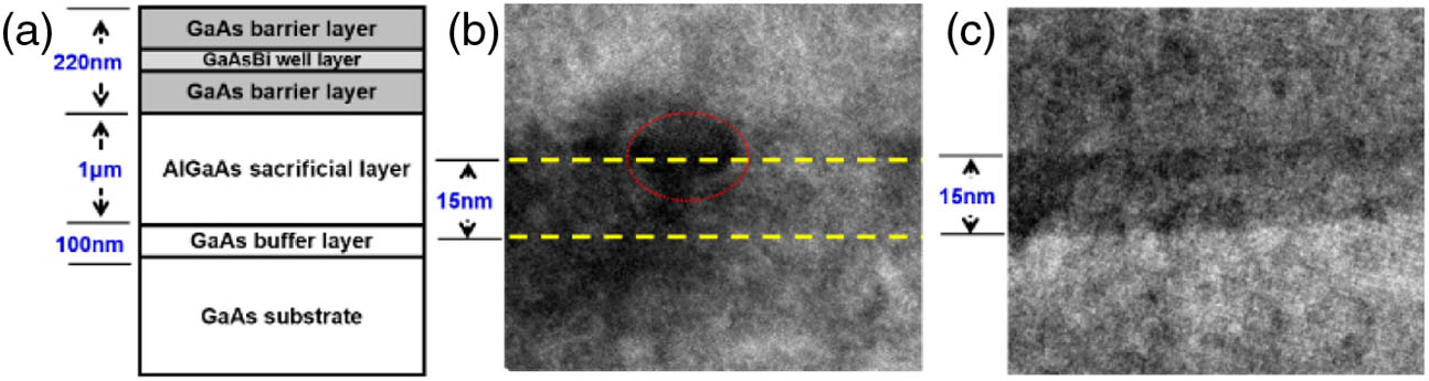
    Fig. 1. (a) Schematic diagram of the GaAsBi/GaAs single QW structure. (b) TEM image showing the as-grown 15 nm thick single GaAsBi/GaAs QW. (c) TEM image showing the same QW after RTA.
    Fabrication process of the GaAsBi microdisk. The electron beam lithography resist Zep520 is directly spin-coated on the wafer, with subsequent inductively coupled plasma-reactive ion etching transferring the disk pattern down to the active layer. Finally, the AlGaAs sacrificial layer is oxidized and then undercut by hydrofluoric acid for the free-standing disk.
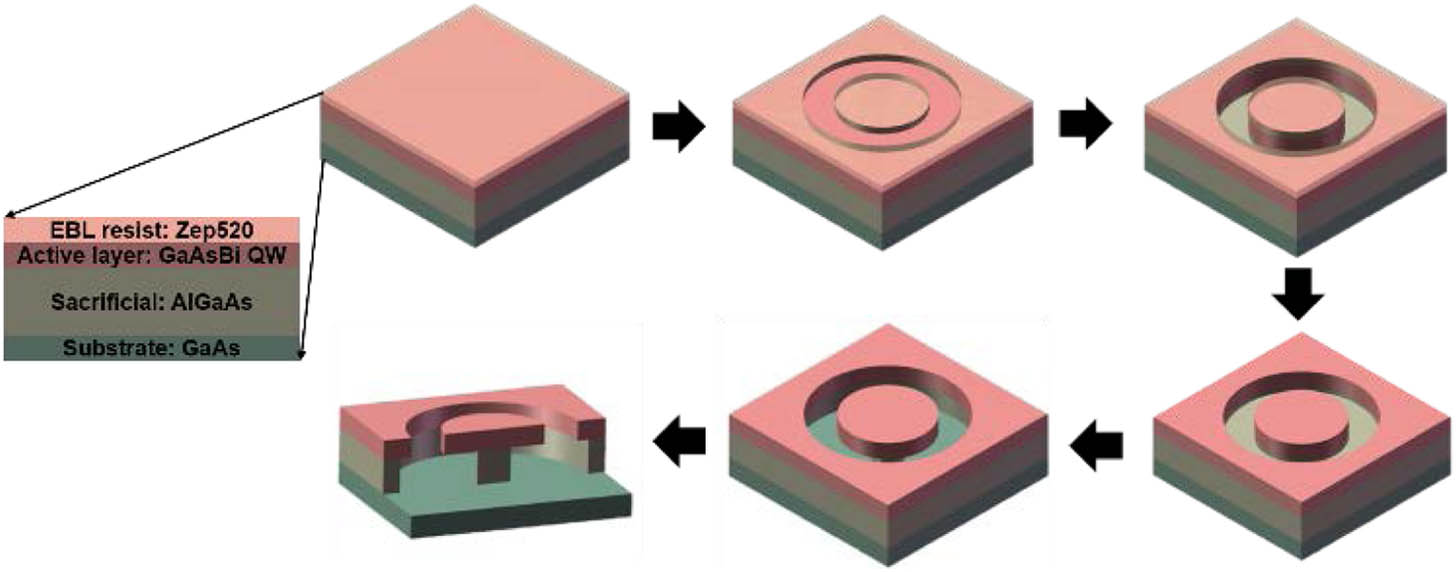
    Fig. 2. Fabrication process of the GaAsBi microdisk. The electron beam lithography resist Zep520 is directly spin-coated on the wafer, with subsequent inductively coupled plasma-reactive ion etching transferring the disk pattern down to the active layer. Finally, the AlGaAs sacrificial layer is oxidized and then undercut by hydrofluoric acid for the free-standing disk.
    (a) Cold disk cavity oscillates with the gain QW structure resulting in the lasing behavior with a good consistency of FSR between theoretical and experimental (pumping of 101.2 μW) results. The inset is the FDTD simulation for mode profiles of lasing wavelengths 1276 nm and 1407 nm, respectively. (b) GaAsBi QW PL well covers the wavelength range from 1100 to 1400 nm. (c) The evolution of PL spectra of the GaAsBi microdisk laser of radius 0.75 μm at various pumping power.
    Fig. 3. (a) Cold disk cavity oscillates with the gain QW structure resulting in the lasing behavior with a good consistency of FSR between theoretical and experimental (pumping of 101.2 μW) results. The inset is the FDTD simulation for mode profiles of lasing wavelengths 1276 nm and 1407 nm, respectively. (b) GaAsBi QW PL well covers the wavelength range from 1100 to 1400 nm. (c) The evolution of PL spectra of the GaAsBi microdisk laser of radius 0.75 μm at various pumping power.
    (a) Scanning electron microscopy images of a fabricated GaAsBi microdisk laser at different radii. (b) The collected PL spectra for the GaAsBi microdisk laser with a radius of 0.75, 1.00, and 1.50 μm with related L–L curves and FWHMs. The chosen peak is indicated by a black arrow. For the smallest radius of 0.75 μm, the lasing threshold is 1.2 μW and the FWHM is 2.5±0.3 nm.
    Fig. 4. (a) Scanning electron microscopy images of a fabricated GaAsBi microdisk laser at different radii. (b) The collected PL spectra for the GaAsBi microdisk laser with a radius of 0.75, 1.00, and 1.50 μm with related L–L curves and FWHMs. The chosen peak is indicated by a black arrow. For the smallest radius of 0.75 μm, the lasing threshold is 1.2 μW and the FWHM is 2.5±0.3  nm.
    YearStructureBi Concentration (%)PumpingCavityLasing Wavelength (nm)Reference
    2010Bulk2.5OP-pulsedFP982.8, 986.2[33]
    2013Bulk4.2OP-pulsedFP1088.6, 1204[34]
    2013QW2.2EP-pulsedFP947[35]
    2014QW6EP-pulsedFP1060[36]
    2014Bulk3, 4EP-pulsedFP976, 1045[37]
    2017QW5.8EP-pulsed & CWFP1142, 1135[28,38]
    2018QW5.8OP-CWMicrodisk1276, 1407This work
    Table 1. Brief Summary of GaAsBi-Based Infrared Lasers
    Xiu Liu, Lijuan Wang, Xuan Fang, Taojie Zhou, Guohong Xiang, Boyuan Xiang, Xueqing Chen, Suikong Hark, Hao Liang, Shumin Wang, Zhaoyu Zhang. Continuous wave operation of GaAsBi microdisk lasers at room temperature with large wavelengths ranging from 1.27 to 1.41  μm[J]. Photonics Research, 2019, 7(5): 508
    Download Citation