Yunlin Chen, Tianwei Fan, Man Tong. Diffractive self-imaging based on selective etching of a ferroelectric domain inversion grating[J]. Chinese Optics Letters, 2015, 13(2): 020502
Copy Citation Text
A hexagonal array grating based on selective etching of a 2D ferroelectric domain inversion in a periodically poled MgO-doped crystal is fabricated. The effects to the diffractive self-imaging as a function of diffraction distance for a fixed phase difference and array duty cycle of the grating is theoretically analyzed. The Talbot diffractive self-imaging properties after selective etching of a 2D ferroelectric domain inversion grating under a fixed phase difference are experimentally demonstrated. A good agreement between theoretical and experimental results is observed.
The phenomenon of self-imaging of periodic objects, also known as the Talbot effect, was first observed by Talbot in 1836[1]. The field diffracted from a periodic object illuminated by a plane wave was found to replicate the object transmittance at certain imaging planes, and has led to a variety of applications in imaging processing and synthesis, photolithography, optical testing, optical metrology, spectrometry, optical computing, as well as in near-field scanning optical microscopy[2]. Particularly, a Talbot interferometer becomes very useful in X-ray imaging due to the lack of efficient lenses for X-rays[3].
The Talbot effect is manifested when a grating is illuminated with a highly spatially coherent plane wave. Self-imaging is possible for periodic or also quasi-periodic objects (i.e., the Montgomery effect[4]). The Talbot effect requires periodic objects, and images are produced solely by free-space propagation of a diffracted optical field at integer multiples of Talbot distances. Different optical elements have been made to exhibit self-imaging based on the Talbot effect[5,6]. Among the various devices, a tunable array can be realized with spatial light modulators (SLMs) based on, for example, liquid crystals. However, a commercial SLM usually has relatively big pixel dimensions, which limits further applications.
A (LN) crystal is a practical material for use in a Talbot phase array (TPA) due to its perfect optical characteristics[7]. However, applying a high external electric field restricts the Talbot diffractive self-imaging (TDSI) based on periodically poled LN (PPLN) to applications in optical integration and optical microstructure devices. PPLN and periodically poled (PPLT) can be used to realize second-harmonic self-imaging from 1D PPLN[8], and second-harmonic Talbot self-imaging from 1D and 2D PPLT[9]. A MgO LN (MgLN) crystal showed a shorter absorption edge and higher resistance to photorefractive damage than that of LN[10]. Moreover, because of it has a lower switching field, periodically poled MgLN (PPMgLN) has been expected to be fairly easily fabricated by means of electric-field poling[11]. These features are important to reduce the applied electric field, and improve TPA performance. A high flexibility for designing a TPA could be obtained if arbitrary surface-relief diffractive optical elements of high quality could be patterned in a MgLN crystal. Ferroelectric domains of opposite spontaneous polarization present different etching speeds when dipped in some acid mixtures. In this work, we theoretically analyzed the effects on TDSI based on 2D surface-relief diffraction grating from a diffraction distance. According to the theoretical simulation, we fabricated a 2D surface-relief diffraction grating based on PPMgLN by selective etching. The TDSI properties of the selective etching of a 2D ferroelectric domain inversion grating under a fixed phase difference are experimentally demonstrated.
Sign up for Chinese Optics Letters TOC. Get the latest issue of Chinese Optics Letters delivered right to you!Sign up now
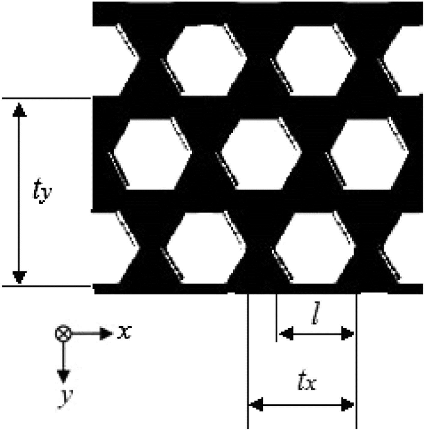
A 2D hexagonal array grating was designed because of its high efficiency with respect to luminous energy utilization and high compatibility with other optical devices. A hexagonal ferroelectric domain inversion grating is shown in Fig. 1, where and are the periods in the and -directions (respectively), and the period , , hexagon width , and duty cycle . An expanded laser with a wavelength of 532 nm is used as the incident light source.
Based on the theory of Fresnel images of plane periodic objects[12], a simple method of hexagonal array illumination based on the Talbot effect was reported[13]. The transmitted field of the hexagonal array structure within a period can be written as . Omitting a common phase factor, can be expressed as where and are positive integers, and can be calculated as where represents the zeroth component. As shown in Fig. 1, for a phase grating, in Ref. [13]
When a hexagonal array grating is illuminated with a monochromatic plane wave, the diffracted field at an arbitrary -imaging plane can be expressed in the following Fourier series expansion
Then we substitute , , and into following equation, where represents the Talbot distance, is the coefficient of the Talbot distance, and is the input wavelength. Then can be rewritten as
Through Eqs. (1)–(5), Fig. 2 shows the simulated TDSI at integer multiples of the Talbot distance and fractional values of the Talbot distance; the phase difference and the duty cycle is 0.56.
Figure 2.Numerical simulation TDSI (for ); (a)–(d) with respect to distance coefficient , 3, 5, and 10; (e)–(h) with respect to distance coefficient , 0.33, 0.50, and 0.70.
From numerical simulations, we knew that the intensity distribution of the TDSI is sensitive to the diffraction distance. The same TDSI is obtained at distances that are integer multiples of the Talbot distance , and the intensity of the diffraction decreases with increasing distance coefficient [as shown in Figs. 2(a)–2(d)]. A TDSI that is more complex occurs at fractional values of the Talbot distance [14,15] as shown in Figs. 2(e)–2(h).
A MgLN substrate allows light transmission over a wide spectral range, from the IR to the UV regions (5 μm–350 nm). The sample was cut from a c-cut, optically polished, 1.0 mm thick wafer obtained from a 5 mol.% MgO doping congruent LN crystal. A 2D grating of periodically inverted ferroelectric domains, along the axis, in a MgLN sample, was obtained by photolithographic and electric field poling processes. The periodic domain reversal poling process is shown in Fig. 3, which consists of three sections: an incubation stage, a poling stage, and a stabilization stage.
Figure 3.Waveform for the 2D ferroelectric domain inversion MgLN.
The pitch of this hexagonal pattern is 25 μm. After poling, the sample was etched to obtain a ferroelectric domain inversion grating. In fact, more than 2 h of etching in a 90°C acid mixture results in differential etching of the opposite ferroelectric domain faces. In this way we obtain a 2D pattern in which each hexagonal domain became a truncated pyramid. The ferroelectric patterns were obtained in large areas () as required for photonics applications. Figure 4(a) shows an optical microscope image of the domains’ inversion patterns after the poling process, whereas Fig. 4(b) represents a scanning electron microscope (SEM) image of the obtained sample after the etching process. The sample had a duty cycle around 56% and a microstructure height of about 20 μm.
Spatially resolved micro-Raman spectroscopy was employed to investigate possible perturbations in the local structure of the crystalline material after polarization reversal[16,17]. The obtained spectra collected at the center of the original (no poling) inverted regions are shown in Fig. 5. As observed, little differences can be detected either in the position of the Raman peaks or in the spectral widths, the obtained spectra being identical. That is, no structural changes are observed which means that our poling process is a suitable technique to produce domain-inverted structures in MgLN crystals.
Figure 5.Raman spectra collected at the original (noninverted) and domain inverted areas.
We used a MgLN-based 2D (hexagonal) array of periodically inverted ferroelectric domains with a duty cycle 56%, and a pitch of size of 25 and 20 μm in depth, of a MgLN sample for studying TDSI. To this aim a simple optical setup was used, as depicted in Fig. 6. A diode laser operating at a wavelength of 532 nm illuminated the sample. For the 2D array sample, the Talbot distance is , where is the period of the hexagonal grating. The laser beam was remodeled by a double-lens telescope system in order to obtain a smaller laser spot size. When the plane wave propagates along the axis to the sample, the TDSI will be magnified by a microscope objective and recorded by a CCD camera. The distance between the sample and microscope objective is the diffraction distance. In order to investigate the influence of the diffraction distance on the self-imaging patterns, the phase difference was fixed at .
Figure 6.Experimental setup of diffraction self-imaging.
The TDSI patterns were recorded by a CCD camera. Pictures of the TDSI patterns obtained are shown in Fig. 7. The diffraction patterns in Figs. 7(a)–7(d) were recorded when , 3, 5, and 10, and the patterns in Figs. 7(e)–7(h) were recorded when , 0.33, 0.50, and 0.70. It is obvious that the same TDSI is obtained at distances that are integer multiples of the Talbot distance , and the TDSI with a high intensity-contrast is obtained with the distance coefficient is decreased [as shown in Figs. 7(a)–7(d)]. A variety of interesting TDSIs have been obtained at fractional values of the Talbot distance [as shown in Figs. 7(e)–7(h)]. The experiment results showed that the self-imaging patterns changed with the diffraction distance as the phase difference was fixed, which verified the numerical calculation results.
Figure 7.Experimental TDSI patterns obtains (); (a)–(d) on , 3, 5, and 10 planes; (e)–(h) on , 0.33, 0.50, and 0.70 planes.
In conclusion, we theoretically and experimentally study the TDSI of a 2D ferroelectric domain inversion grating based on selective etching of MgLN. Theoretical simulations are done for effects to the TDSI as a function of the diffraction distance for a fixed phase difference and array duty cycle of the grating. On the basis of the theoretical results, we fabricate a 2D hexagonal ferroelectric domain inversion array with duty cycle based on selective etching of PPMgLN. The TDSI properties after selective etching of a 2D ferroelectric domain inversion grating under a fixed phase difference are experimentally demonstrated. The work reported in this Letter shows that a TDSI with a high intensity-contrast is obtained when the distance coefficient decreases in proportion to integer multiples of the Talbot distance , and a variety of TDSIs are obtained at fractional values of the Talbot distance .
Yunlin Chen, Tianwei Fan, Man Tong. Diffractive self-imaging based on selective etching of a ferroelectric domain inversion grating[J]. Chinese Optics Letters, 2015, 13(2): 020502