• Acta Optica Sinica
  • Vol. 43, Issue 5, 0509001 (2023)
Siqin Tao, Ming Kong, Wei Liu*, Jianan Xu, Fuxia Cheng, Kaixuan Liu, and Zeqiu Yang
Author Affiliations
  • College of Metrology and Measurement Engineering, China Jiliang University, Hangzhou 310018, Zhejiang, China
  • show less
    DOI: 10.3788/AOS221540 Cite this Article Set citation alerts
    Siqin Tao, Ming Kong, Wei Liu, Jianan Xu, Fuxia Cheng, Kaixuan Liu, Zeqiu Yang. Microchannel Detection Based on Dual-Wavelength Image-Plane Digital Holographic Microscopy[J]. Acta Optica Sinica, 2023, 43(5): 0509001 Copy Citation Text show less
    Schematic of experimental apparatus
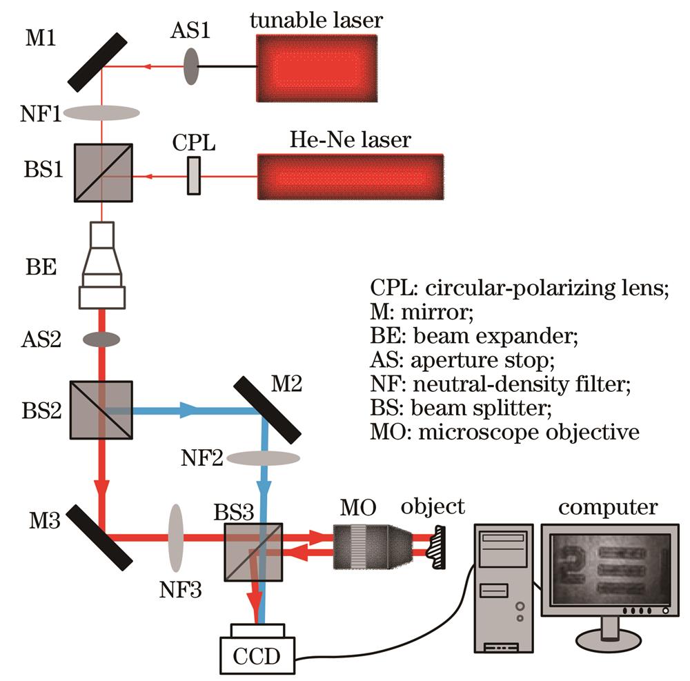
    Fig. 1. Schematic of experimental apparatus
    Magnification calibration experimental results. (a) Test target 1951 USAF pattern; (b) element intensity image of group 6; (c) locally magnified intensity image of the 5th pair of lines
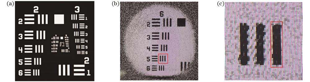
    Fig. 2. Magnification calibration experimental results. (a) Test target 1951 USAF pattern; (b) element intensity image of group 6; (c) locally magnified intensity image of the 5th pair of lines
    Schematic of micro-nano one-dimensional grid structure
    Fig. 3. Schematic of micro-nano one-dimensional grid structure
    Experimental results of transverse resolution calibration. (a) Reproduction phase of group 7 element in the resolution target; (b) phase reproduction of grid with 5 μm line width; (c) phase image reproduction of grid with 1 μm line width
    Fig. 4. Experimental results of transverse resolution calibration. (a) Reproduction phase of group 7 element in the resolution target; (b) phase reproduction of grid with 5 μm line width; (c) phase image reproduction of grid with 1 μm line width
    Measurement results of segment difference standard film. (a) Depth image; (b) height graph
    Fig. 5. Measurement results of segment difference standard film. (a) Depth image; (b) height graph
    Chip physical diagram and structure diagram. (a) PDMS chip physical diagram; (b) PDMS chip channel at 50× magnification; (c) enlargement structure diagram of silicon substrate chip channel
    Fig. 6. Chip physical diagram and structure diagram. (a) PDMS chip physical diagram; (b) PDMS chip channel at 50× magnification; (c) enlargement structure diagram of silicon substrate chip channel
    Straight channel holograms under different wavelengths. (a) 632.8 nm channel hologram; (b) 632.8 nm reference hologram; (c) 635.32 nm channel hologram; (d) 635.32 nm reference hologram
    Fig. 7. Straight channel holograms under different wavelengths. (a) 632.8 nm channel hologram; (b) 632.8 nm reference hologram; (c) 635.32 nm channel hologram; (d) 635.32 nm reference hologram
    Wrapped phase images of straight channel. (a) Wrapped phase for 632.8 nm; (b) wrapped phase for 635.32 nm; (c) equivalent wavelength phase distribution
    Fig. 8. Wrapped phase images of straight channel. (a) Wrapped phase for 632.8 nm; (b) wrapped phase for 635.32 nm; (c) equivalent wavelength phase distribution
    Straight channel measurement results. (a) Depth image; (b) three-dimensional topography image; (c) compare experimental result
    Fig. 9. Straight channel measurement results. (a) Depth image; (b) three-dimensional topography image; (c) compare experimental result
    Circular chamber measurement results. (a) Depth image; (b) three-dimensional topography image; (c) sectional graph
    Fig. 10. Circular chamber measurement results. (a) Depth image; (b) three-dimensional topography image; (c) sectional graph
    Silicon substrate chip measurement results. (a) Depth image; (b) three-dimensional topography image; (c) sectional graph
    Fig. 11. Silicon substrate chip measurement results. (a) Depth image; (b) three-dimensional topography image; (c) sectional graph
    Measurement methodWidth /μmDepth /μm
    Dual-wavelength digital holography75.848.6
    White light interferometry78.750.0
    Table 1. Comparison of three-dimensional topography measurement results of microfluidic chip straight channel
    Measurement methodWidth /μmDepth /μm
    Dual-wavelength digital holography76.648.5
    White light interferometry78.950
    Table 2. Comparison of three-dimensional topography measurement results of circular chamber channels in microfluidic chips
    Siqin Tao, Ming Kong, Wei Liu, Jianan Xu, Fuxia Cheng, Kaixuan Liu, Zeqiu Yang. Microchannel Detection Based on Dual-Wavelength Image-Plane Digital Holographic Microscopy[J]. Acta Optica Sinica, 2023, 43(5): 0509001
    Download Citation