Abstract
We study through electromagnetic modeling the absorption of light of a given wavelength in an array of horizontal InP nanowires of diameter less than 100 nm. Such absorption is performed most efficiently by using polarized light and by exciting a coupled optical resonance in a sparse array. In that case, we excite a resonance in the individual nanowires and couple the resonances in neighboring nanowires through a lattice resonance of the periodic array. At such a resonance, an array with nanowires of 80 nm in diameter can absorb more than eight times more strongly than a tight-packed array, despite containing a seven times smaller amount of the absorbing InP material.Nanophotonics and photonic crystalsIII–V semiconductor nanowires are popular for many optoelectronic applications [1,2], including photodetection [3,4]. Nanowires allow for miniaturized single-nanowire detectors as well as for large-area detectors when the nanowires are placed next to each other [3,5]. Furthermore, small-diameter nanowires allow, due to strain relaxation in the radial direction, for a much larger freedom in the combination of lattice mismatched materials than in a conventional thin-film layer [6–9]. Such material freedom allows, through ternary III–V compounds [10], for the engineering of the bandgap in photodetection applications. The detection of photons is at the heart of current high-speed optical communication. There, a matching of the bandgap wavelength to the communication wavelength is desirable. Such a matching typically leads to a higher signal-to-noise ratio in the detection by suppressing the dark current in the photodetector [11].
Thus, we would like to enhance the absorption of light in the vicinity of the bandgap wavelength in small-diameter nanowires. For that purpose, we use here three properties common for nanostructures. First, single nanostructures can show optical resonances whose wavelength position depends on the size and shape of the structure [12–19]. Second, periodic nanostructures can show period-dependent lattice resonances that originate from the diffractive coupling between the constituent structures [12,13,20]. Third, coupling between these two types of resonances can show up, which has been identified in metallic systems [13,21].
However, such coupling of resonances has not been studied in absorbing horizontal nanowire arrays [22–24]. Here, we show that the optical resonances in individual horizontal nanowires [1] can couple with lattice resonances, leading to absorption peaks. We use an array of InP nanowires embedded in as a model system. We show that the best way to absorb photons of a given wavelength in nanowires of diameter less than 100 nm is to use polarized light and to excite a coupled resonance. For a diameter of 80 nm, the nanowires can absorb 30% of the incident photons when the coupled resonance is excited. In this case, the nanowires absorb eight times more strongly than a tight-packed array of nanowires, despite consisting of a seven times smaller amount of InP. The resonance becomes stronger and narrower when the diameter decreases toward 50 nm, for which an absorptance of 50% can be reached. In case a higher absorptance is required, we need to turn to nanowires with diameter exceeding 100 nm.
Sign up for Photonics Research TOC. Get the latest issue of Photonics Research delivered right to you!Sign up now
We consider InP nanowires of diameter placed in an array of period and surrounded by glass of refractive index (Fig. 1). Light is incident at a normal angle to the array to maximize the projected area of the array to the incident light. TM (TE) polarized incident light has the electric field parallel (perpendicular) to the axis of the nanowires. We perform the modeling with a scattering matrix method [25] that solves the Maxwell’s equations for the light scattering for a given wavelength . To describe the optical response of the InP material in the nanowires, we use tabulated values [26] for the complex-valued refractive index whose imaginary part gives rise to absorption in the material. We calculate the reflectance and the transmittance of the array. From these, the absorptance of the nanowires can be obtained.
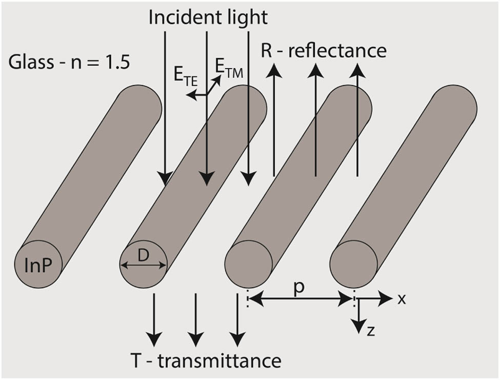
Figure 1.Periodic array of horizontal InP nanowires embedded in a glass matrix of refractive index . The period is and the nanowire diameter is . Light is incident at a normal angle to the array and either TE or TM polarized. Notice that we show here four of the infinitely many nanowires of the array. Furthermore, we assume in the modeling that each nanowire is infinitely long.
We consider light of in wavelength, which is in the vicinity of 925 nm, the bandgap wavelength [10] of InP. Note that we use [26] in the modeling. We start with the case of a rather dense array with a fixed diameter to period ratio of (Fig. 2). We find that TM polarized light is absorbed considerably more strongly than TE polarized light. This polarization behavior can actually be understood from an electrostatic model. The incident electric field of TE polarized light of is screened from the interior of each nanowire by a factor of [4,27]. Thus, the electric field in the interior of each nanowire shows the magnitude of . In contrast, TM polarized light does not experience such screening, and in this case [4]. Since the local absorption in each nanowire is proportional to , we expect a factor of stronger absorption for TM polarized light. Actually, we can calculate analytically the absorptance of the nanowire array under this electrostatic approximation. Notice that the irradiance of the incident light is given by [27]. Therefore, the power that is incident into a unit cell of period is given by . Next, the local absorption, that is, the ohmic heating, is given by [27]. Therefore, the absorption in a unit cell, which occurs in a nanowire of cross-section area , is given by . Consequently, the absorptance in this electrostatic approximation is given by . We find here for good agreement between the full electromagnetic modeling and this electrostatic approximation (solid versus dashed lines in Fig. 2). Notice that even for the stronger absorbed TM polarized light, the absorptance reaches values of just 5% at a diameter of 100 nm.

Figure 2.Absorptance at in a horizontal array of InP nanowires for a fixed period to diameter ratio of . Here, results from full electromagnetic modeling (solid lines) as well as from an electrostatic approximation (dashed lines) are shown for both TE and TM polarized incident light.
However, we know from previous studies that individual nanowires of should show a resonance for TM polarized incident light at [1]. By solving for the eigenmodes [1] in individual nanowires, we expect the mode to show up for at . Indeed, when we fix the period to to study a sparse array where we expect to possibly see the response of the individual nanowires, we find an absorption peak at for TM polarized light (Fig. 3). Regarding the behavior of the eigenmodes, notice that the mode in individual, isolated nanowires shows symmetry in the polar direction (inset in Fig. 3). This follows from the fact that the first index in the mode labeling, in or , defines the polar dependence of the form [1]. Furthermore, in the periodic array, we find an absorption peak for both TM and TE polarized light at . These peaks are caused by the and eigenmodes in the individual nanowires, which are expected to show up for from our calculation on individual, isolated nanowires. Notice that the mode will not show any dependence in the polar direction. In contrast, the mode will show two nodes along the polar direction due to the dependence.
Figure 3.Absorptance at in a horizontal nanowire array of period for both TE and TM polarized incident light. The arrows indicate peaks that arise from resonances in the individual nanowires. The inset shows the field distribution of the eigenmode in an individual nanowire, as calculated also in [1]. The eigenmode shows up for , and the dashed circle denotes the nanowire.
Thus, to investigate if we can increase the absorptance beyond the 5% value for (Fig. 2), we choose and vary (Fig. 4). For TE polarized light, drops with increasing . This drop is a signature that the collection area of incident light is limited for each nanowire, and more light “slips” through the array with increasing , as seen in the inset of Fig. 4, where and with increasing . In strong contrast, when increases from 80 to 400 nm for TM polarized light, the absorptance does not drop from the value of 4%. Even more interestingly, the absorptance shows a very pronounced peak of at . Thus, the nanowire array absorbs eight times more strongly in this sparse configuration compared to the case of a tight-packed array of , where the array contains seven times more InP. We note here that the reflectance of TM polarized light shows a peak at and a dip at (see inset in Fig. 4). Such a peak–dip pair resembles the behavior of a high-contrast grating where a Fano resonance, characterized by a peak–dip pair, shows up due to the interference between the normally incident light and an in-plane resonance of the grating [28,29]. Thus, we have reason to believe that the absorption peak in Fig. 4 arises due to the excitation of an in-plane resonance in the nanowire array.
Figure 4.Absorptance for both TE and TM polarized incident light at in a horizontal nanowire array with nanowires of diameter . The inset shows the reflectance and transmittance for both polarizations.
To understand the behavior of this absorption peak at , we show in Fig. 5(a) the dependence of the absorptance on both and . We find that the peak shifts to a smaller diameter with increasing period. Thus, by tuning the period, we find an absorption peak even for nanowires of just 50 nm in diameter. Actually, the resonance becomes stronger at compared to at , and increases from 30% to 50%. We assign this absorption peak to a coupled resonance between the resonance and a lattice resonance. The lattice resonance shows here up at a period of where the first diffracted order couples the light scattered between neighboring nanowires. We note that we have found similar, but weaker, peaks whenever , where the th diffracted order couples neighboring nanowires (not shown).
Figure 5.Absorptance as a function of nanowire diameter and array period for (a) TM and (b) TE polarized light at . The dashed lines denote the diameter where the , , and resonances [1] show up in a single nanowire for .
We show in Fig. 6(a) the electric field distribution for and and in Fig. 6(b) for and , which is at the coupled mode resonance. For , we see predominantly the excitation of the mode in the individual nanowires, without noticeable coupling between the nanowires [see Fig. 6(c) for a schematic]. The field pattern here follows closely that of the eigenmode solved for an individual, isolated nanowire (inset in Fig. 3). In contrast, at , we see how light is scattered between neighboring nanowires through the lattice resonance [see Fig. 6(d) for a schematic]. Due to this coupling of the resonance between neighboring nanowires, the intensity in each nanowire is enhanced by an order of magnitude over that in the case of above, leading consecutively to the enhancement in absorption by a factor of 8 in Fig. 4.
Figure 6. for TM polarized light in the plane at for a period of (a) and (b) . Here, three nanowires of 80 nm in diameter are shown (dashed circles). Light is incident from the top side with and a region of 600 nm in length both above and below the nanowire array is shown. Notice the difference in the color scale by a factor of 10 between (a) and (b). (c) Schematic of the resonance in the individual nanowires in (a). (d) Schematic of the coupled resonance between the resonance and the lattice resonance in (b).
Regarding the coupling between nanowires, actually, at , we find that (Fig. 4) for TM polarized light. Further analysis showed that here (see inset in Fig. 4). Thus, the nanowires can become transparent to the incident light. This Wood’s anomaly [20] shows up as follows. Part of the incident light scatters from the nanowires into the first diffracted order, which propagates in the plane of the array, that is, in the -direction, when . Also this first diffracted order is TM polarized, and it is excited in such a way that it is out of phase with the incident light at the location of the nanowires (not shown here). Therefore, the electric field at the location of the nanowires reaches low values, leading to and .
We notice that there is a peak in the absorptance for TM polarized light also at [Fig. 5(a)], but this peak does not shift noticeably with period . We attribute this peak to the mode and the weak dependence on the period to a weaker scattering of the mode compared to the mode in individual nanowires (not shown), which leads to weaker excitation of the lattice resonance.
We note that no peaks show up in for TE polarized light for [Fig. 5(b)]. For this polarization, to maximize , it is best to use a tight-packed array with , but even then, the absorptance is limited to . However, if we allow for , we find also for TE polarized light an absorption resonance that shifts toward smaller diameters with increasing . We attribute this peak to coupling between the mode, which is expected at , and the lattice resonance. In this case can be reached.
We note that our results on the coupled mode resonance are not exclusive for a wavelength in the immediate vicinity of the bandgap wavelength. We have found similar results for InP nanowires at for example , 700, and 800 nm. Also, we expect the coupled resonance to be a property of the nanowire geometry and the array period, and therefore not strongly dependent on the exact choice of the direct bandgap III–V semiconductor material. Furthermore, we have found that when the nanowires are placed on a glass substrate, the coupled mode resonance shows up. In this case, the resonance shows increasing strength as the nanowires are covered by a glass layer of increasing thickness to resemble the case of nanowires fully embedded in glass, as considered above.
We note that in experiments, nanowires of a finite length are considered. A detailed study of the impact of the nanowire length on the coupled resonance is beyond the scope of this study. However, we have found indication that the optical response of nanowires of length equal to five times the wavelength starts to resemble closely the response of infinitely long nanowires.
In conclusion, we have shown in the linear optical regime that the optimum way to absorb light of a given wavelength in an array of horizontal InP nanowires of diameter less than 100 nm is to use coupled optical resonances. By carefully tuning the nanowire diameter and the array period, resonances in the individual nanowires can couple between neighboring nanowires through a lattice resonance.
References
[1] L. Cao, J. S. White, J.-S. Park, J. A. Schuller, B. M. Clemens, M. L. Brongersma. Engineering light absorption in semiconductor nanowire devices. Nat. Mater., 8, 643-647(2009).
[2] J. Wallentin, N. Anttu, D. Asoli, M. Huffman, I. Åberg, M. H. Magnusson, G. Siefer, P. Fuss-Kailuweit, F. Dimroth, B. Witzigmann, H. Q. Xu, L. Samuelson, K. Deppert, M. T. Borgström. InP nanowire array solar cells achieving 13.8% efficiency by exceeding the ray optics limit. Science, 339, 1057-1060(2013).
[3] L. Vj, J. Oh, A. P. Nayak, A. M. Katzenmeyer, K. H. Gilchrist, S. Grego, N. P. Kobayashi, W. Shih-Yuan, A. A. Talin, N. K. Dhar, M. S. Islam. A perspective on nanowire photodetectors: current status, future challenges, and opportunities. IEEE J. Quantum Electron., 17, 1002-1032(2011).
[4] J. Wang, M. S. Gudiksen, X. Duan, Y. Cui, C. M. Lieber. Highly polarized photoluminescence and photodetection from single indium phosphide nanowires. Science, 293, 1455-1457(2001).
[5] H. Kind, H. Yan, B. Messer, M. Law, P. Yang. Nanowire ultraviolet photodetectors and optical switches. Adv. Mater., 14, 158-160(2002).
[6] G. Kästner, U. Gösele. Stress and dislocations at cross-sectional heterojunctions in a cylindrical nanowire. Philos. Mag., 84, 3803-3824(2004).
[7] M. S. Gudiksen, L. J. Lauhon, J. Wang, D. C. Smith, C. M. Lieber. Growth of nanowire superlattice structures for nanoscale photonics and electronics. Nature, 415, 617-620(2002).
[8] M. T. Björk, B. J. Ohlsson, T. Sass, A. I. Persson, C. Thelander, M. H. Magnusson, K. Deppert, L. R. Wallenberg, L. Samuelson. One-dimensional steeplechase for electrons realized. Nano Lett., 2, 87-89(2002).
[9] Y. Wu, R. Fan, P. Yang. Block-by-block growth of single-crystalline Si/SiGe superlattice nanowires. Nano Lett., 2, 83-86(2002).
[10] I. Vurgaftman, J. R. Meyer, L. R. Ram-Mohan. Band parameters for III–V compound semiconductors and their alloys. J. Appl. Phys., 89, 5815-5875(2001).
[11] B. E. A. Saleh, M. C. Teich. Fundamentals of Photonics(2007).
[12] F. J. García de Abajo. Colloquium: light scattering by particle and hole arrays. Rev. Mod. Phys., 79, 1267-1290(2007).
[13] B. Auguié, W. L. Barnes. Collective resonances in gold nanoparticle arrays. Phys. Rev. Lett., 101, 143902(2008).
[14] R. Paniagua-Dominguez, G. Grzela, J. G. Rivas, J. A. Sanchez-Gil. Enhanced and directional emission of semiconductor nanowires tailored through leaky/guided modes. Nanoscale, 5, 10582-10590(2013).
[15] L. Novotny, N. van Hulst. Antennas for light. Nat. Photonics, 5, 83-90(2011).
[16] N. Anttu, H. Q. Xu. Efficient light management in vertical nanowire arrays for photovoltaics. Opt. Express, 21, A558-A575(2013).
[17] S.-K. Kim, R. W. Day, J. F. Cahoon, T. J. Kempa, K.-D. Song, H.-G. Park, C. M. Lieber. Tuning light absorption in core/shell silicon nanowire photovoltaic devices through morphological design. Nano Lett., 12, 4971-4976(2012).
[18] B. Wang, P. W. Leu. Tunable and selective resonant absorption in vertical nanowires. Opt. Lett., 37, 3756-3758(2012).
[19] L. Zhou, X. Q. Yu, J. Zhu. Metal-core/semiconductor-shell nanocones for broadband solar absorption enhancement. Nano Lett., 14, 1093-1098(2014).
[20] A. Hessel, A. A. Oliner. A new theory of Wood’s anomalies on optical gratings. Appl. Opt., 4, 1275-1297(1965).
[21] E. M. Hicks, S. Zou, G. C. Schatz, K. G. Spears, R. P. Van Duyne, L. Gunnarsson, T. Rindzevicius, B. Kasemo, M. Käll. Controlling plasmon line shapes through diffractive coupling in linear arrays of cylindrical nanoparticles fabricated by electron beam lithography. Nano Lett., 5, 1065-1070(2005).
[22] D. Tham, J. R. Heath. Ultradense, deep subwavelength nanowire array photovoltaics as engineered optical thin films. Nano Lett., 10, 4429-4434(2010).
[23] S. K. Kim, K. D. Song, T. J. Kempa, R. W. Day, C. M. Lieber, H. G. Park. Design of nanowire optical cavities as efficient photon absorbers. ACS Nano, 8, 3707-3714(2014).
[24] L. Y. Cao, P. Y. Fan, A. P. Vasudev, J. S. White, Z. F. Yu, W. S. Cai, J. A. Schuller, S. H. Fan, M. L. Brongersma. Semiconductor nanowire optical antenna solar absorbers. Nano Lett., 10, 439-445(2010).
[25] N. Anttu, H. Q. Xu. Scattering matrix method for optical excitation of surface plasmons in metal films with periodic arrays of subwavelength holes. Phys. Rev. B, 83, 165431(2011).
[26] O. J. Glembocki, E. D. Palik, H. Piller. Indium phosphide (InP). Handbook of Optical Constants of Solids, 503-516(1997).
[27] N. Anttu. Geometrical optics, electrostatics, and nanophotonic resonances in absorbing nanowire arrays. Opt. Lett., 38, 730-732(2013).
[28] Y. Zhou, M. Moewe, J. Kern, M. C. Huang, C. J. Chang-Hasnain. Surface-normal emission of a high-Q resonator using a subwavelength high-contrast grating. Opt. Express, 16, 17282-17287(2008).
[29] Z. Ye, M. C. Y. Huang, C. Chase, V. Karagodsky, M. Moewe, B. Pesala, F. G. Sedgwick, C. J. Chang-Hasnain. High-index-contrast grating (HCG) and its applications in optoelectronic devices. IEEE J. Sel. Top. Quantum Electron., 15, 1485-1499(2009).


