Chengli Wang, Jiachen Cai, Liping Zhou, Ailun Yi, Bingcheng Yang, Yuanhao Qin, Jiaxiang Zhang, Xin Ou. Progress of Silicon Carbide Integrated Photonics[J]. Acta Optica Sinica, 2023, 43(16): 1623017
Search by keywords or author
- Acta Optica Sinica
- Vol. 43, Issue 16, 1623017 (2023)
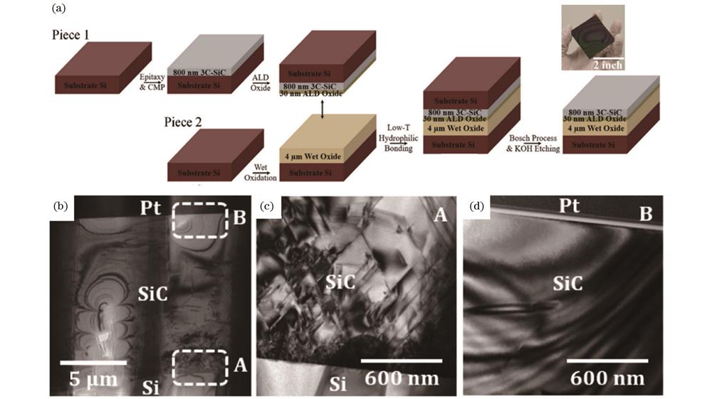
![Fabrication of 3C-SiCOI based on heteroepitaxy, wafer bonding, and grinding thinning methods[35-36]. (a) Preparation process; (b) SEM image of each layer of 3C-SiCOI; (c) TEM image of area A in the SEM image, showing more lattice defects at the initial epitaxial interface; (d) TEM image of region B in the SEM image, showing that the lattice is intact at the bonding interface](/richHtml/gxxb/2023/43/16/1623017/img_01.jpg)
Fig. 1. Fabrication of 3C-SiCOI based on heteroepitaxy, wafer bonding, and grinding thinning methods[35-36]. (a) Preparation process; (b) SEM image of each layer of 3C-SiCOI; (c) TEM image of area A in the SEM image, showing more lattice defects at the initial epitaxial interface; (d) TEM image of region B in the SEM image, showing that the lattice is intact at the bonding interface
![Fabrication of 4H-SiCOI based on ion implantation and transfer method[37]. (a) Preparation process; (b) photo of the prepared 4H-SiCOI; (c) lattice recovery of the SiC layer through the annealing process; (d) SEM image of each layer of 4H-SiCOI; (e) TEM image of 4H-SiCOI](/richHtml/gxxb/2023/43/16/1623017/img_02.jpg)
Fig. 2. Fabrication of 4H-SiCOI based on ion implantation and transfer method[37]. (a) Preparation process; (b) photo of the prepared 4H-SiCOI; (c) lattice recovery of the SiC layer through the annealing process; (d) SEM image of each layer of 4H-SiCOI; (e) TEM image of 4H-SiCOI
Fig. 3. Fabrication of 4H-SiCOI based on grinding and thining method[39]. (a) Preparation process; (b) photo of the prepared 4H-SiCOI; (c) uniformity characterization of the 4H-SiCOI film; (d) photo of the prepared 4H-SiCOI with an area of 10 mm×12 mm
Fig. 4. Second harmonic generation in SiCOI[38, 42]. (a) Schematic of a two-dimensional silicon carbide photonic crystal used for second harmonic generation; (b) photonic crystal taken by an optical microscope, the above picture is the fundamental mode at 1502.58 nm taken by an InGaAs camera, the below picture shows the second harmonic generation at 751.3 nm captured by Si CCD; (c) relationship between the output second harmonic power and the pump light power in the photonic crystal; (d) SEM image of silicon carbide microring resonant cavity; (e) phase matching design in the microring; (f) relationship between the output second harmonic power and the pump light power in the microring resonator
Fig. 5. Integrated electro-optic modulator in SiCOI[54-56]. (a) Schematic of the structure of 4H-SiCOI electro-optic modulator; (b) Q value of the microring cavity and the tuning change of the resonance peak with the applied voltage; (c) schematic of the structure of 3H-SiCOI electro-optic modulator; (d) SEM image of the racetrack cavity structure and the tuning variation of the resonance peak with the applied voltage; (e) 3C-SiCOI electro-optic modulator structure; (f) high power operation characterization of 3C-SiCOI electro-optic modulator
Fig. 6. Generation of optical frequency combs in 4H-SiCOI[39, 41-42, 49]. (a) SEM image of 4H-SiCOI microring cavity; (b) generation of silicon carbide soliton optical frequency comb, whose spectrum corresponds to single soliton; (c) SEM image of 4H-SiCOI micro-disk cavity, double soliton and single soliton spectra, and analysis of its noise characteristics; (d) SEM image of 4H-SiCOI microring cavity used for frequency doubling optical frequency comb generation and spectrum of frequency doubling optical frequency comb
Fig. 7. Frequency conversion in 4H-SiCOI mid-infrared frequency comb to visible light frequency comb[39, 64-65]. (a) Optical microscope photo and schematic of the conversion principle when the visible light frequency comb is generated; (b) Q value analysis of silicon carbide in the visible light band; (c) specific process of frequency conversion from infrared frequency comb to visible light frequency comb
Fig. 8. Schematic of the atomic structure of VSi, DV, and NV color centers in 4H-SiC[29]
Fig. 9. Integration of color centers and microcavities in 4H-SiC[42, 50]. (a) SEM image of 4H-SiC one-dimensional photonic crystal; (b) tuning process of cavity mode by nitrogen condensation; (c) life test of VSi color center luminescence in cavity mode; (d) SEM image of 4H-SiC one-dimensional photonic crystal and schematic of its DV color center; (e) spectral comparison between DV luminescence and cavity mode coupling and no coupling; (f) ODMR measurement of DV color center in the microcavity, the picture shows the degeneration in the Rabi oscillation coherent process
Fig. 10. Properties of VSi centers and control over nuclear spin qubits in 4H-SiC triangle waveguide[74]. (a) Schematic of color center produced by He-ion implantation; (b) SEM image of 4H-SiC suspended waveguide, the inset shows the simulation result of the mode distribution of the waveguide; (c) spin coherence of VSi implanted in the waveguide; (d) schematic of coupled electron-nuclear spin triplet state in the waveguide; (e) CPMG sequence testing the modulation and resonance effect of nuclear spin on electron spin; (f) manipulation demonstration of nuclear spin N2 in Bloch sphere
Fig. 11. Color centers of UV pulse laser in silicon carbide nanophotonic cavities[76]. (a) Schematic of photonic crystal microcavity and spectra before and after UV pulse irradiation; (b) spatial intensity distribution of color centers produced by irradiation
Fig. 12. Prospects for the application of SiCOI in integrated nonlinear and quantum photonics[42, 69, 77]. (a) Using multiple color center light sources for quantum state measurement, and using microring resonators for frequency conversion and regulation of color center light sources; (b) single-chip photonic network implementation scheme based on silicon carbide
|
Table 1. Comparison of main performance parameters between typical photonic integrated platforms
|
Table 2. Optical loss comparison between several SiCOI photonic platform
|
Table 3. Main performance comparison of several color centers in 4H-SiC

Set citation alerts for the article
Please enter your email address


