
Yangguang Xing, Lin Li, Jilong Peng, Shanshan Wang, Yinuo Cheng. Optical Design of 3-Order Solar Extreme Ultraviolet Narrowband Slitless Imaging Spectrometer[J]. Acta Optica Sinica, 2021, 41(7): 0730003
- Acta Optica Sinica
- Vol. 41, Issue 7, 0730003 (2021)
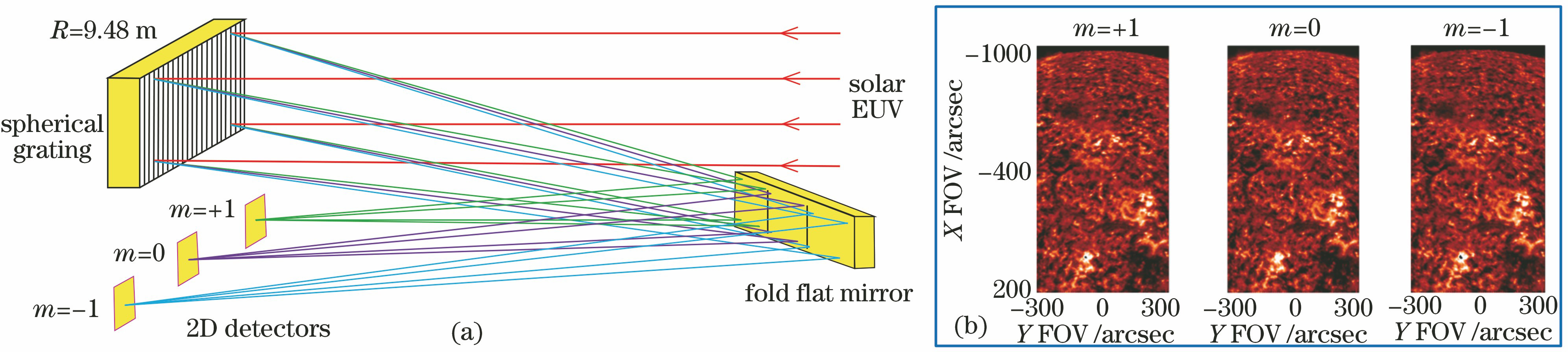
Fig. 1. Schematic of three-order slitless imaging spectrometer. (a) Optical layout of MOSES; (b) solar images with three diffraction orders by single snapshot
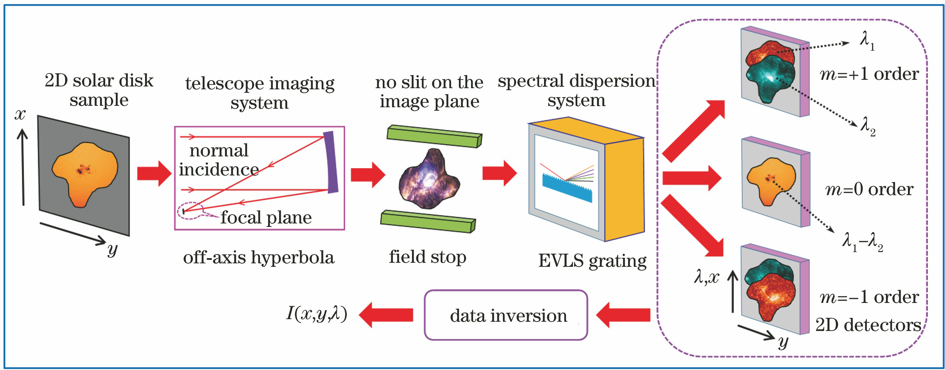
Fig. 2. Schematic of three-order slitless imaging spectrometer with new optical layout
Fig. 3. Ray-tracing model for three-order slitless imaging spectrometer
Fig. 4. Geometric optics model for off-axis hyperbolic mirror
Fig. 5. Schematic of aberration-corrected EVLS grating
Fig. 6. Sun flare spectrum from SDO/EVE
Fig. 7. Optical layout of solar EUV slitless imaging spectrometer. (a) 2D optical layout; (b) 3D model diagram
Fig. 8. Ruling density distribution of EVLS grating
Fig. 9. Curve of aberration term of astigmatisms. (a) Tangential astigmatism for -1 order; (b) tangential astigmatism for +1 order; (c) sagittal astigmatism for -1 order; (d) sagittal astigmatism for +1 order
Fig. 10. Curve of aberration term of coma. (a) Coma for -1 order; (b) coma for +1 order
Fig. 11. Maximum grid distortion change with wavelength under marginal FOV. (a) -1 order; (b) +1 order
Fig. 12. Variation of RMS radius of spot for -1 order. (a) RMS radius of spot versus wavelength in the different off-axis FOVs; (b) RMS radius of spot versus FOV in the different wavelength
Fig. 13. Variation of RMS radius of spot for +1 order. (a) RMS radius of spot versus wavelength in the different off-axis FOVs; (b) RMS radius of spot versus FOV in the different wavelength
Fig. 14. Spot diagrams in 0 order imaging plane under the different FOVs and RMS radius of spot versus FOV for 0 order. (a) Spot diagrams in 0 order imaging plane under the different FOVs; (b) RMS radius of spot versus FOV for 0 order
Fig. 15. MTFs of design system under different diffraction orders. (a) -1 order; (b) +1 order; (c) 0 order
Fig. 16. Diffraction enclosed energy to evaluate system’s spatial resolution. (a) -1 order; (b) +1 order; (c) 0 order
Fig. 17. Spectral resolution simulation verification for ±1 diffraction orders. (a)(b) -1 order; (c)(d) +1 order
Fig. 18. Transmission of Si filter with 0.1 μm thickness
Fig. 19. Reflectance versus wavelength for SiC/Mg multilayer
Fig. 20. Efficiency versus wavelength for EVLS grating
Fig. 21. Effective area of slitless imaging spectrometer versus wavelength
|
Table 1. Specifications of the solar EUV slitless imaging spectrometer
|
Table 2. Fjk terms with their associate aberrations
| ||||||||||||||||||||||||||||||||||||||||||||||||||||||||||||||||||||||||||||||||||||||||||||||||||||||||||||||||||||||||||||||||||||
Table 3. Specifications and optical element parameters for slitless imaging spectrometer
|
Table 4. Periodic SiC/Mg multilayer parameters

Set citation alerts for the article
Please enter your email address
© Copyright 2018-2021 | Chinese Laser Press. All Rights Reserved 沪ICP备15018463号-20