• Laser & Optoelectronics Progress
  • Vol. 58, Issue 22, 2209001 (2021)
Zeyu Wang1、2、3, Chenchen Li1、2, YiQiang Gao1, Hao Sun1, Minghui Yang1, and Xiaowei Sun1、*
Author Affiliations
  • 1Key Laboratory of Terahertz Solid-State Technology, Shanghai Institute of Microsystem and Information Technology, Chinese Academy of Sciences, Shanghai 200050, China
  • 2University of Chinese Academy of Sciences, Beijing, 100049, China
  • 3School of Information Science and Technology, ShanghaiTech University, Shanghai, 201210, China
  • show less
    DOI: 10.3788/LOP202158.2209001 Cite this Article Set citation alerts
    Zeyu Wang, Chenchen Li, YiQiang Gao, Hao Sun, Minghui Yang, Xiaowei Sun. Optimal Design of Heterojunction AlGaAs/GaAs PIN Diode Millimeter-Wave Switch and Its Imaging Application[J]. Laser & Optoelectronics Progress, 2021, 58(22): 2209001 Copy Citation Text show less
    Structure of millimeter wave security inspection imaging system. (a) Core components; (b) transmitting front-end module
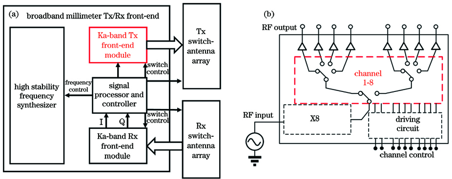
    Fig. 1. Structure of millimeter wave security inspection imaging system. (a) Core components; (b) transmitting front-end module
    Transmission line models and performance curves of grounded coplanar waveguides and microstrip structures. (a) Three-dimensional simulation structure; (b) comparison of simulation results of S parameters
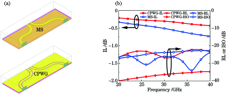
    Fig. 2. Transmission line models and performance curves of grounded coplanar waveguides and microstrip structures. (a) Three-dimensional simulation structure; (b) comparison of simulation results of S parameters
    Two-port equivalent circuit. (a) Bonding wires; (b) equivalent “T” type network with compensation of high-low impedance line
    Fig. 3. Two-port equivalent circuit. (a) Bonding wires; (b) equivalent “T” type network with compensation of high-low impedance line
    Schematic and performance curves of transmission line before and after high-low impedance line compensation. (a) Before compensation; (b) after compensation; (c) comparison of simulation results of S parameters
    Fig. 4. Schematic and performance curves of transmission line before and after high-low impedance line compensation. (a) Before compensation; (b) after compensation; (c) comparison of simulation results of S parameters
    Switch chip evaluation board. (a) SP4T switch; (b) SPDT switch
    Fig. 5. Switch chip evaluation board. (a) SP4T switch; (b) SPDT switch
    Simulation and measurement results of S parameters of different chips. (a) SPDT switch chip evaluation board; (b) SP4T switch chip evaluation board
    Fig. 6. Simulation and measurement results of S parameters of different chips. (a) SPDT switch chip evaluation board; (b) SP4T switch chip evaluation board
    Layout and performance curves of 8-channel switch subcircuits. (a) Actual assembly photograph; (b) simulation results of S parameters under different channels
    Fig. 7. Layout and performance curves of 8-channel switch subcircuits. (a) Actual assembly photograph; (b) simulation results of S parameters under different channels
    Octave frequency multiplier structure and spectrum simulation curves. (a) Chain block diagram; (b) harmonic simulation results
    Fig. 8. Octave frequency multiplier structure and spectrum simulation curves. (a) Chain block diagram; (b) harmonic simulation results
    Schematic and performance curves of wideband bandpass filter. (a) 3D models and; (b) Simulation results of S parameters
    Fig. 9. Schematic and performance curves of wideband bandpass filter. (a) 3D models and; (b) Simulation results of S parameters
    Test framework for transmitting front-end
    Fig. 10. Test framework for transmitting front-end
    Measured results of transmitting front-end module. (a) Output power of each channel and isolation between channels; (b) harmonic rejection
    Fig. 11. Measured results of transmitting front-end module. (a) Output power of each channel and isolation between channels; (b) harmonic rejection
    Schematic of imaging experiment and experimental results. (a) Schematic of imaging scene; (b) original image of active millimeter wave imaging
    Fig. 12. Schematic of imaging experiment and experimental results. (a) Schematic of imaging scene; (b) original image of active millimeter wave imaging
    PerformanceSPDT switchSP4T switch
    Reverse breakdown voltage /V2525
    P1dB /dBm>30>21
    Operation frequency /GHz24--4022--40
    Port return loss /dB2020
    Insertion loss /dB0.70--0.901.10--1.25
    Isolation /dBSize /(mm×mm)402.5×1.0352.0×1.5
    Table 1. Overall performance of SPDT and SP4T switches
    Zeyu Wang, Chenchen Li, YiQiang Gao, Hao Sun, Minghui Yang, Xiaowei Sun. Optimal Design of Heterojunction AlGaAs/GaAs PIN Diode Millimeter-Wave Switch and Its Imaging Application[J]. Laser & Optoelectronics Progress, 2021, 58(22): 2209001
    Download Citation