• Journal of Semiconductors
  • Vol. 42, Issue 11, 112101 (2021)
Yuming Xue, Shipeng Zhang, Dianyou Song, Liming Zhang, Xinyu Wang, Lang Wang, and Hang Sun
Author Affiliations
  • Tianjin Key Laboratory of Film Electronic & Communication Devices, School of Electronics Information Engineering, Tianjin University of Technology, Tianjin 300384, China
  • show less
    DOI: 10.1088/1674-4926/42/11/112101 Cite this Article
    Yuming Xue, Shipeng Zhang, Dianyou Song, Liming Zhang, Xinyu Wang, Lang Wang, Hang Sun. Effect of concentration of cadmium sulfate solution on structural, optical and electric properties of Cd1–xZnxS thin films[J]. Journal of Semiconductors, 2021, 42(11): 112101 Copy Citation Text show less
    SEM images of Cd1–xZnxS thin films prepared with different concentrations of cadmium sulfate.
    Fig. 1. SEM images of Cd1–xZnxS thin films prepared with different concentrations of cadmium sulfate.
    (Color online) Element distribution diagrams of Cd1–xZnxS thin films deposited with different concentrations of cadmium sulfate.
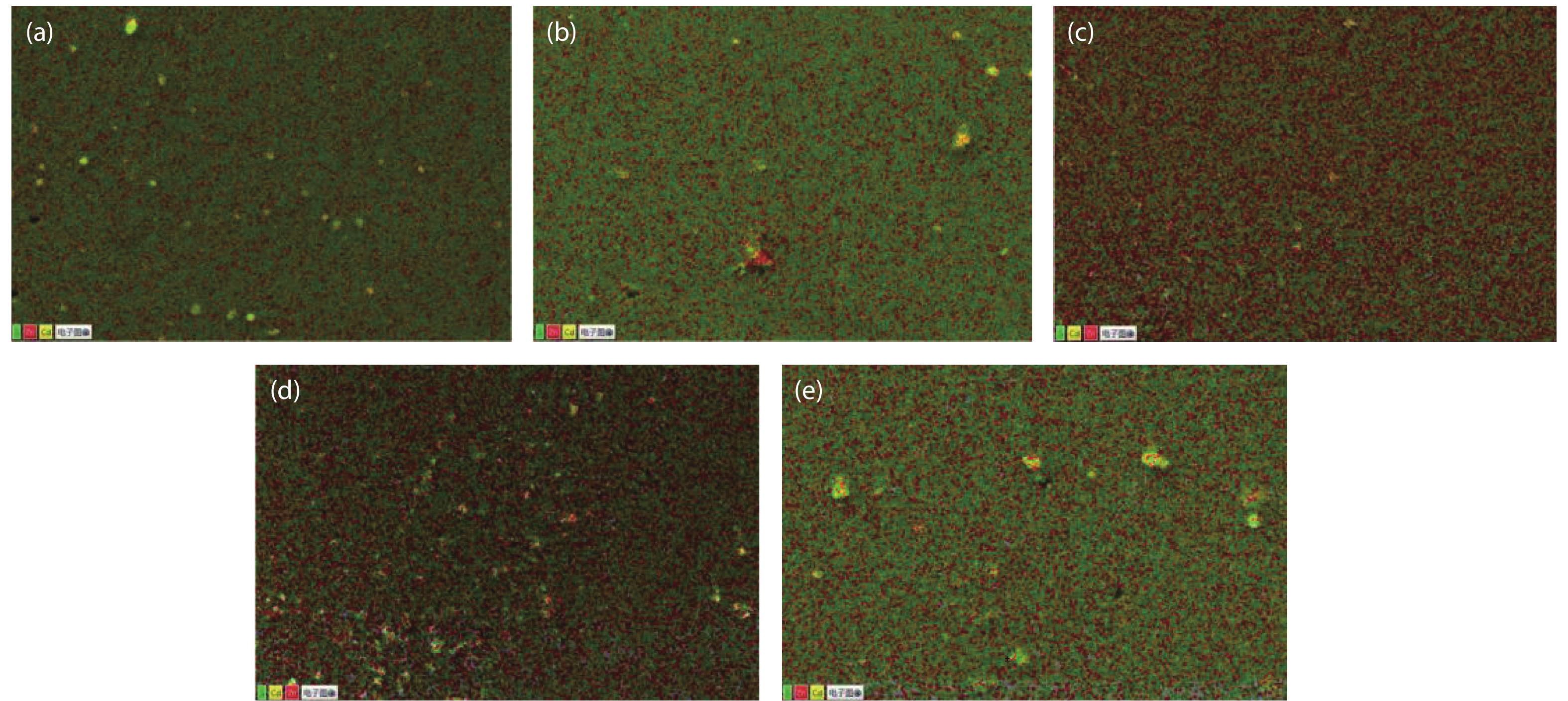
    Fig. 2. (Color online) Element distribution diagrams of Cd1–xZnxS thin films deposited with different concentrations of cadmium sulfate.
    XRD patterns of Cd1–xZnxS thin films deposited at different concentrations of cadmium sulfate.
    Fig. 3. XRD patterns of Cd1–xZnxS thin films deposited at different concentrations of cadmium sulfate.
    Plots of (a) absorbance vs wavelength and (b) transmittance vs wavelength for the Cd1–xZnxS thin films prepared with different concentrations of cadmium sulfate.
    Fig. 4. Plots of (a) absorbance vs wavelength and (b) transmittance vs wavelength for the Cd1–xZnxS thin films prepared with different concentrations of cadmium sulfate.
    Band gap of Cd1–xZnxS thin films deposited with different concentrations of cadmium sulfate.
    Fig. 5. Band gap of Cd1–xZnxS thin films deposited with different concentrations of cadmium sulfate.
    The value of Cd1–xZnxS thin film band gap changes with x.
    Fig. 6. The value of Cd1–xZnxS thin film band gap changes with x.
    ReagentConcentration (M)
    ZnSO40.020
    (NH4)2SO40.025
    SC(NH2)20.015
    NH3·H2O 25%
    CdSO40.003, 0.004, 0.005, 0.006, 0.007
    Table 1. Deposition conditions of CBD-Cd1–xZnxS.
    Concentration of cadmium sulfate (M)Thickness (nm)
    0.00371.13
    0.00473.28
    0.00564.73
    0.00662.46
    0.00766.51
    Table 2. Thickness of Cd1–xZnxS thin films with different cadmium sulfate concentration.
    Concentration of cadmium sulfate (M)Atom ratio of S, Zn and CdZn/(Zn+Cd)
    0.00330.40 : 36.81 : 32.790.529
    0.00431.87 : 34.34 : 33.790.504
    0.00522.17 : 55.83 : 22.000.717
    0.00622.61 : 57.24 : 20.150.739
    0.00728.82 : 37.92 : 33.260.533
    Table 3. The atom ratios of S, Zn and Cd in Cd1–xZnxS thin films prepared with different concentrations of cadmium sulfate.
    Cd (at.%)Zn (at.%)S (at.%)Zn/CdCd1–xZnxS Eg (eV)
    32.7936.8130.401.12Cd0.48Zn0.52S 2.95
    33.7934.3431.871.02Cd0.50Zn0.50S 2.93
    22.0055.8322.172.54Cd0.28Zn0.72S 3.24
    20.1557.2422.612.84Cd0.26Zn0.74S 3.27
    33.2637.9228.821.14Cd0.47Zn0.53S 2.97
    Table 4. Film element content, zinc-cadmium content ratio and band gap.
    Yuming Xue, Shipeng Zhang, Dianyou Song, Liming Zhang, Xinyu Wang, Lang Wang, Hang Sun. Effect of concentration of cadmium sulfate solution on structural, optical and electric properties of Cd1–xZnxS thin films[J]. Journal of Semiconductors, 2021, 42(11): 112101
    Download Citation